Semiconductor device and manufacturing method

a technology of semiconductors and manufacturing methods, applied in the direction of semiconductor devices, basic electric elements, electrical appliances, etc., can solve the problem of reducing the threshold voltage of a mis-hemt, and achieve the effect of mitigating the reduction of the threshold voltag

Inactive Publication Date: 2010-02-25
OKI ELECTRIC IND CO LTD
View PDF1 Cites 54 Cited by
  • Summary
  • Abstract
  • Description
  • Claims
  • Application Information

AI Technical Summary

Benefits of technology

[0011]An object of the present invention is to provide the gate insulation film in a MIS-HEMT having a recessed str

Problems solved by technology

The presence of a gate insulation film between the substrate and the gate electrode,

Method used


Image

  • Semiconductor device and manufacturing method
  • Semiconductor device and manufacturing method
  • Semiconductor device and manufacturing method

Examples


Embodiment Construction

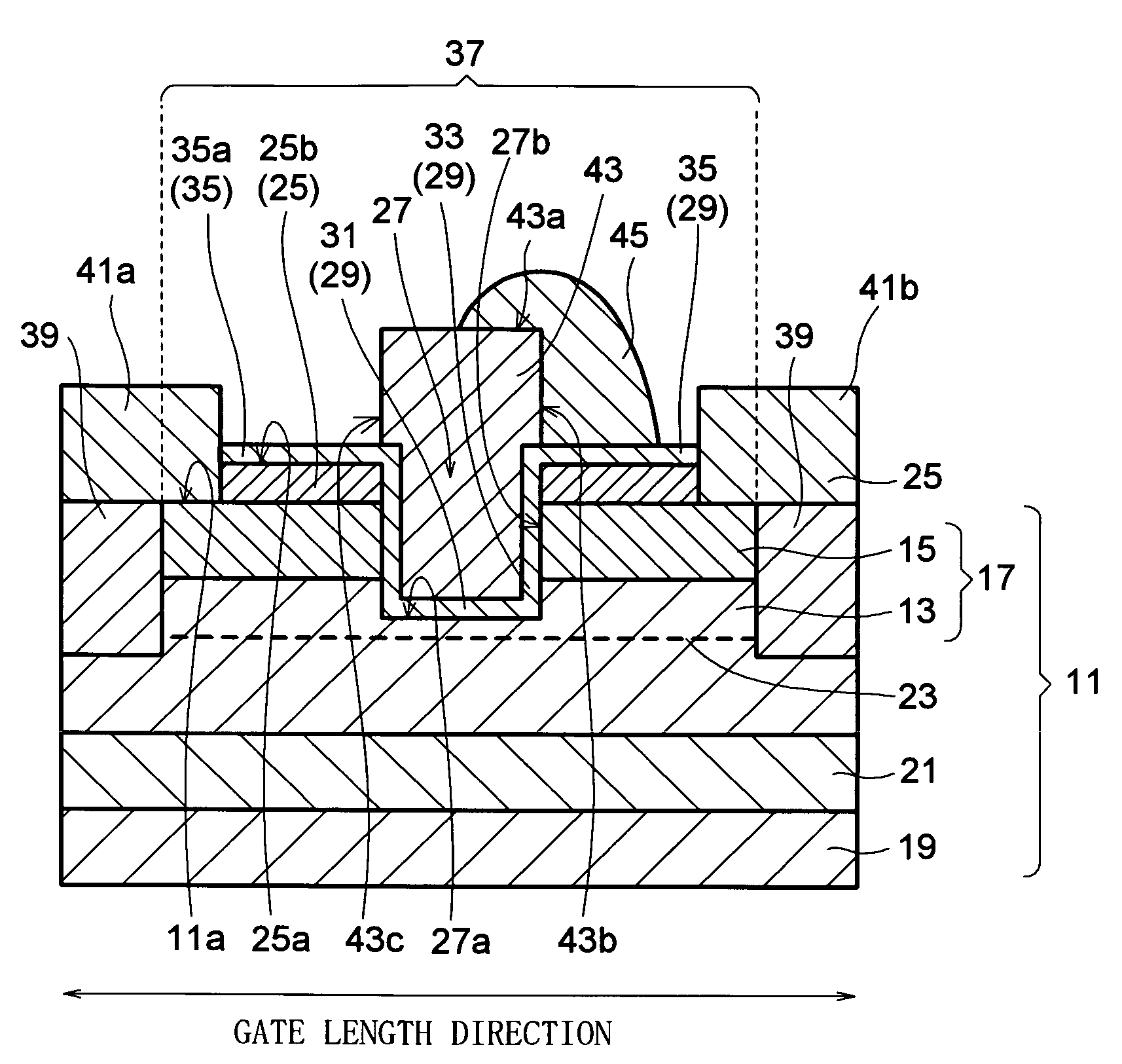
[0030]A MIS-HEMT and fabrication method embodying the present invention, will now be described with reference to the attached non-limiting drawings, in which like elements are indicated by like reference characters.

[0031]The inventive MIS-HEMT has the structure summarized above, the gate electrode being formed on a gate insulation film having a crystal density of at least 2.9 g / cm3, in a recess on the surface of the substrate. The inventive MIS-HEMT fabrication method includes the following four steps.

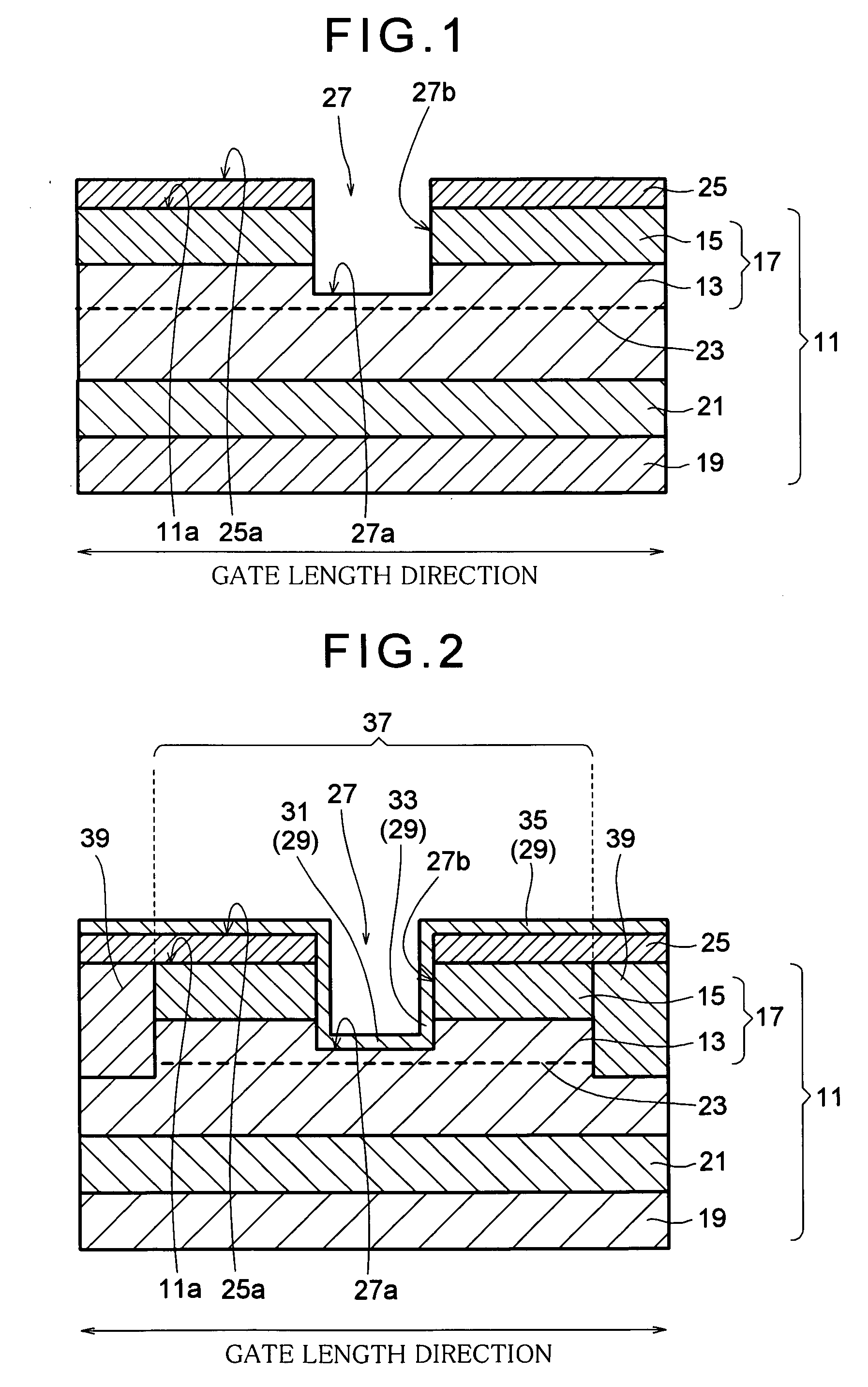
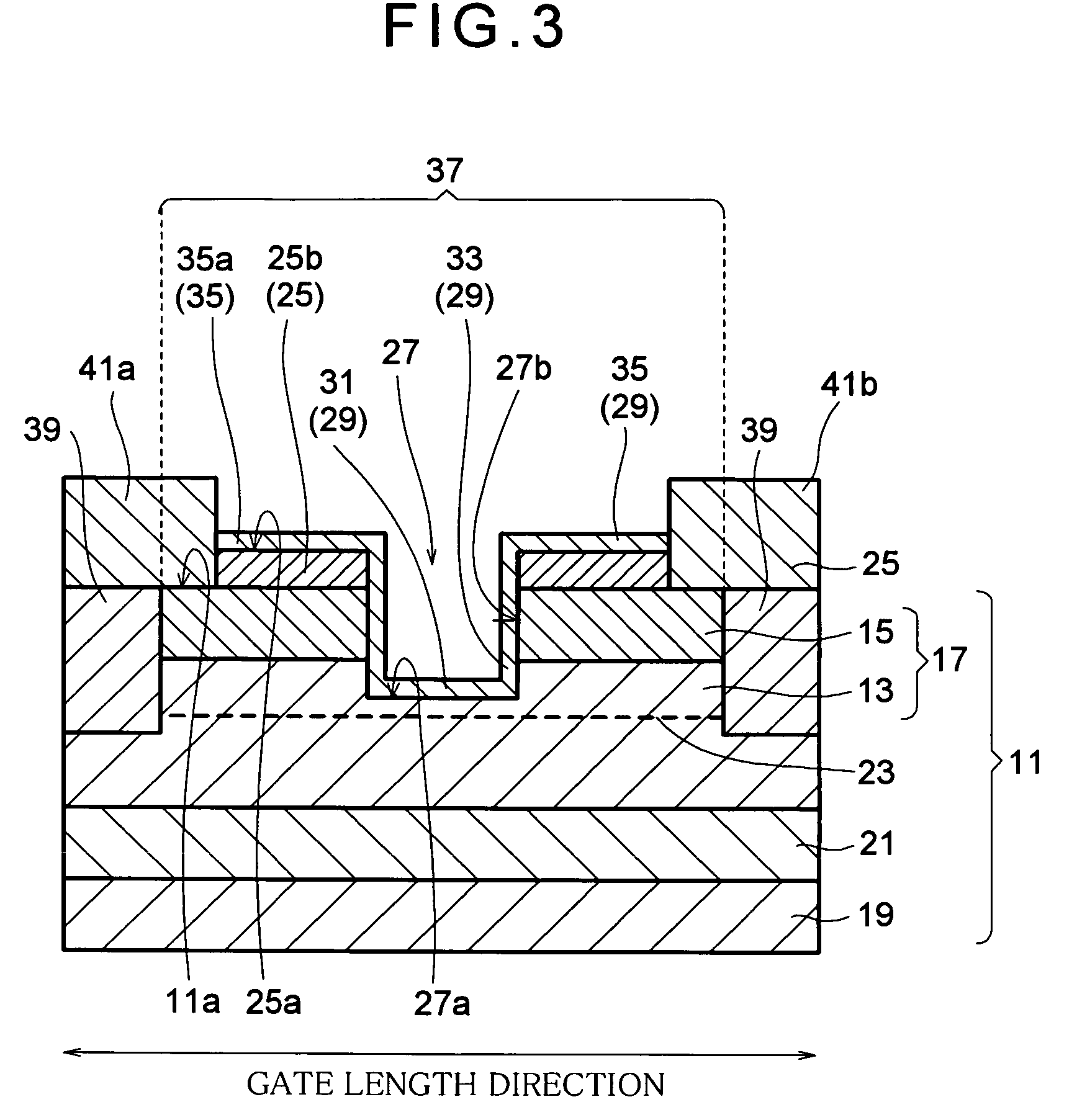
[0032]In the first step, a recess 27 is formed on a major surface 11a of a substrate 11 to obtain the structure shown in FIG. 1. The substrate 11 includes a layered active structure 17 formed on a base layer 19. The layered active structure 17 includes the electron channel layer and electron supply layer.

[0033]The substrate of the MIS-HEMT may in general be a silicon substrate, a silicon-on-insulator (SOI) substrate, or a semiconductor substrate of various other known types, as called ...


PUM


Abstract

A metal-insulator-semiconductor high electron mobility transistor (MIS-HEMT) has a substrate in which an electron supply layer is interposed between an electron channel layer and the surface of the substrate. A pair of main electrodes are formed on the surface of the substrate. A recess is formed in the surface of the substrate between the main electrodes. A gate insulation film is formed on the surface of the substrate, at least between the first and second main electrodes, covering the inside walls and floor of the recess. A gate electrode is formed on the gate insulation film, filling in the recess. The gate insulation film has a crystal density of at least 2.9 g/cm3, which mitigates the reduction in threshold voltage caused by the recess.

Description

BACKGROUND OF THE INVENTION[0001]1. Field of the Invention[0002]The present invention relates to a semiconductor device and a method of manufacturing it, more particularly to a high electron mobility transistor having a metal-insulator-semiconductor structure and a method of manufacturing it.[0003]2. Description of the Related Art[0004]A high electron mobility transistor (HEMT) is a type of field-effect transistor in which current flows in a two-dimensional electron gas (2DEG). One known HEMT structure has a substrate including an undoped gallium nitride (GaN) electron channel layer and an aluminum gallium nitride (AlGaN) electron supply layer. The source, drain, and gate electrodes are disposed on the surface of the AlGaN electron supply layer. A 2DEG layer forms within the electron channel layer by piezo polarization and / or spontaneous polarization of the heterojunction interface between the electron channel layer and the electron supply layer. The electron supply layer has low re...

Claims


Application Information

Patent Timeline
IPC IPC(8): H01L29/778H01L21/335
CPCH01L29/2003H01L29/402H01L29/7787H01L29/518H01L29/66462H01L29/4236
Inventor MARUI, TOSHIHARU
Owner OKI ELECTRIC IND CO LTD
Why Eureka
Try Eureka