Polarization control in VCSELs using photonics crystals

a technology of photonic crystals and polarization control, which is applied in the direction of semiconductor lasers, optical resonator shape and construction, laser details, etc., can solve the problems of polarization of optical beams, thermal heating during operation and the growth or formation of layers, and the inability to meet or achieve the reflectivity requirement of vcsels

Inactive Publication Date: 2007-02-08
II VI DELAWARE INC
View PDF22 Cites 52 Cited by
  • Summary
  • Abstract
  • Description
  • Claims
  • Application Information

AI Technical Summary

Benefits of technology

[0010] Another embodiment includes a method of manufacturing an optical device. The method includes forming a lower mirror on a substrate. An active region is formed on the lower mirror. An upper mirror is formed on the active region. The method further includes forming an asymmetrical photonic crystal that includes cavities. The asymmetrical photonic crystal is optically coupled in the optical device such that one polarization of light is better reflected by the asymmetrical photonic crystal than a competing polarization of light.

Problems solved by technology

The reflectivity requirement of VCSELs typically cannot be satisfied or achieved with metallic mirrors or cleaved semiconductor-to-air interface mirrors.
The large number of DBR layers also increases the electrical resistance of the VCSEL and may lead to problems with both heating during operation and the growth or formation of the layers.
One challenge that exists with the above mentioned devices relates to polarization of optical beams.
Additionally, un-polarized light reflected back into the laser cavity can cause feedback reverberation issues that affect the laser output.
An isolator that works for laser emission without single fixed polarization would be significantly more costly.

Method used


Image

  • Polarization control in VCSELs using photonics crystals
  • Polarization control in VCSELs using photonics crystals
  • Polarization control in VCSELs using photonics crystals

Examples


Embodiment Construction

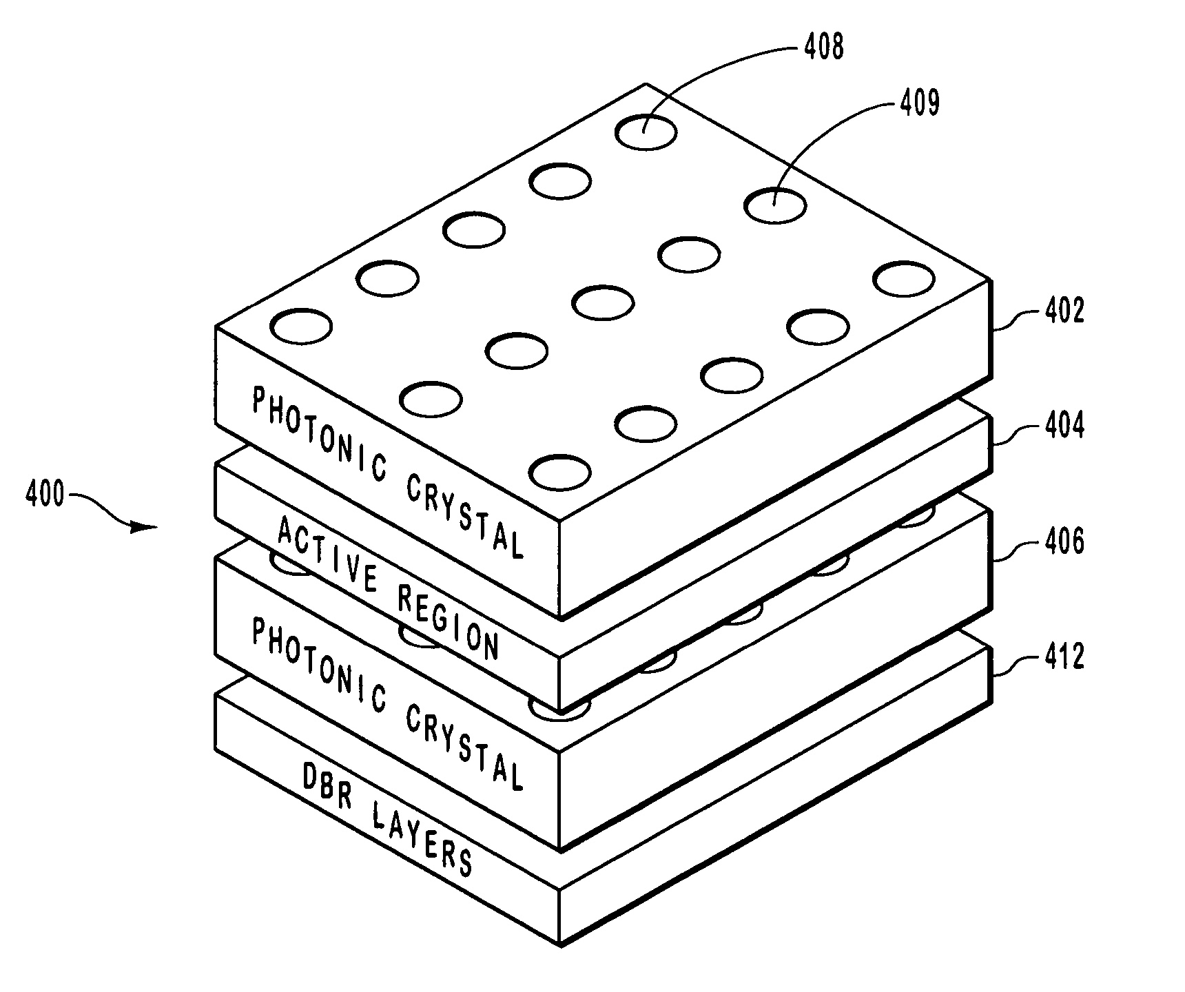
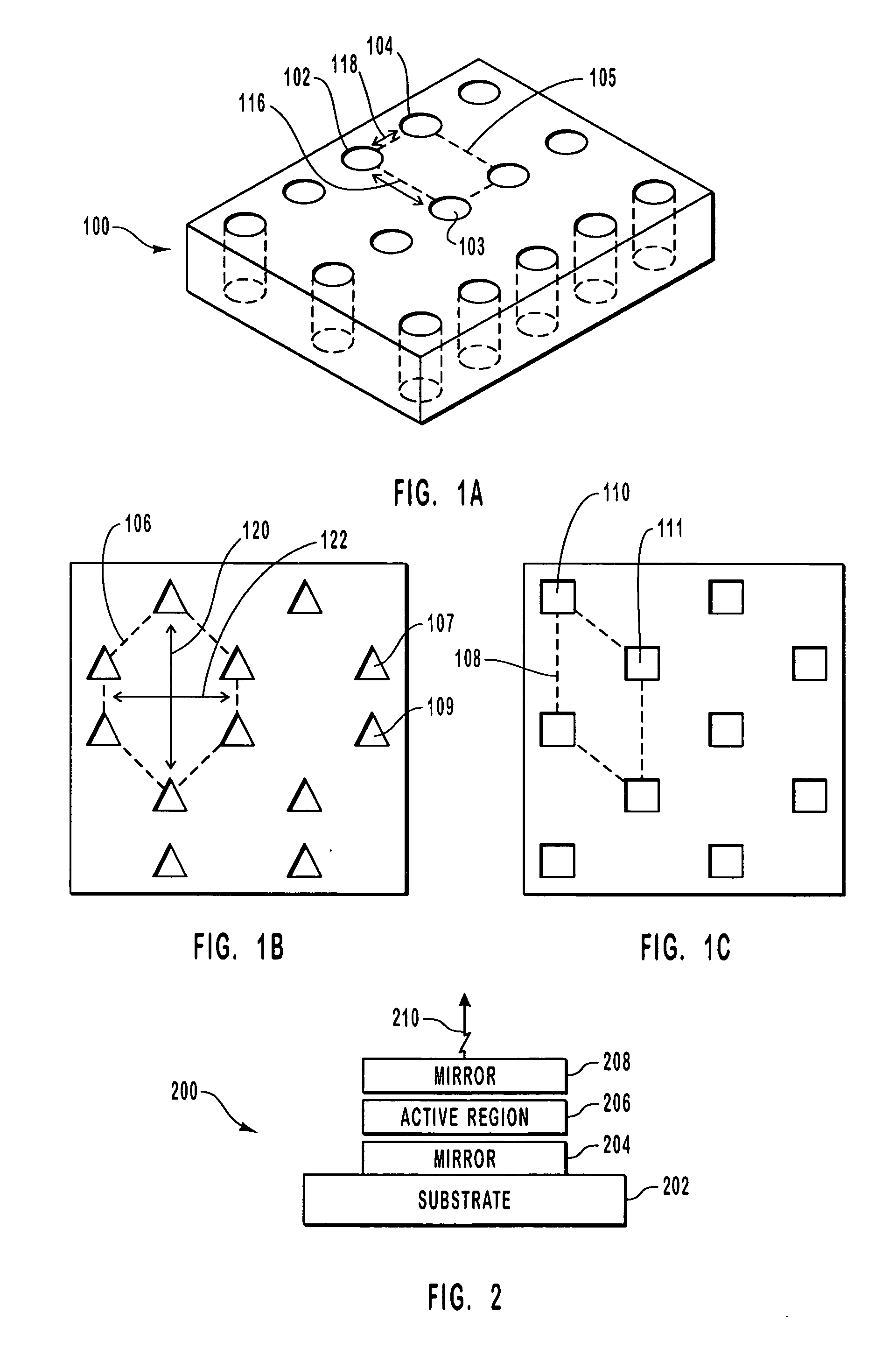
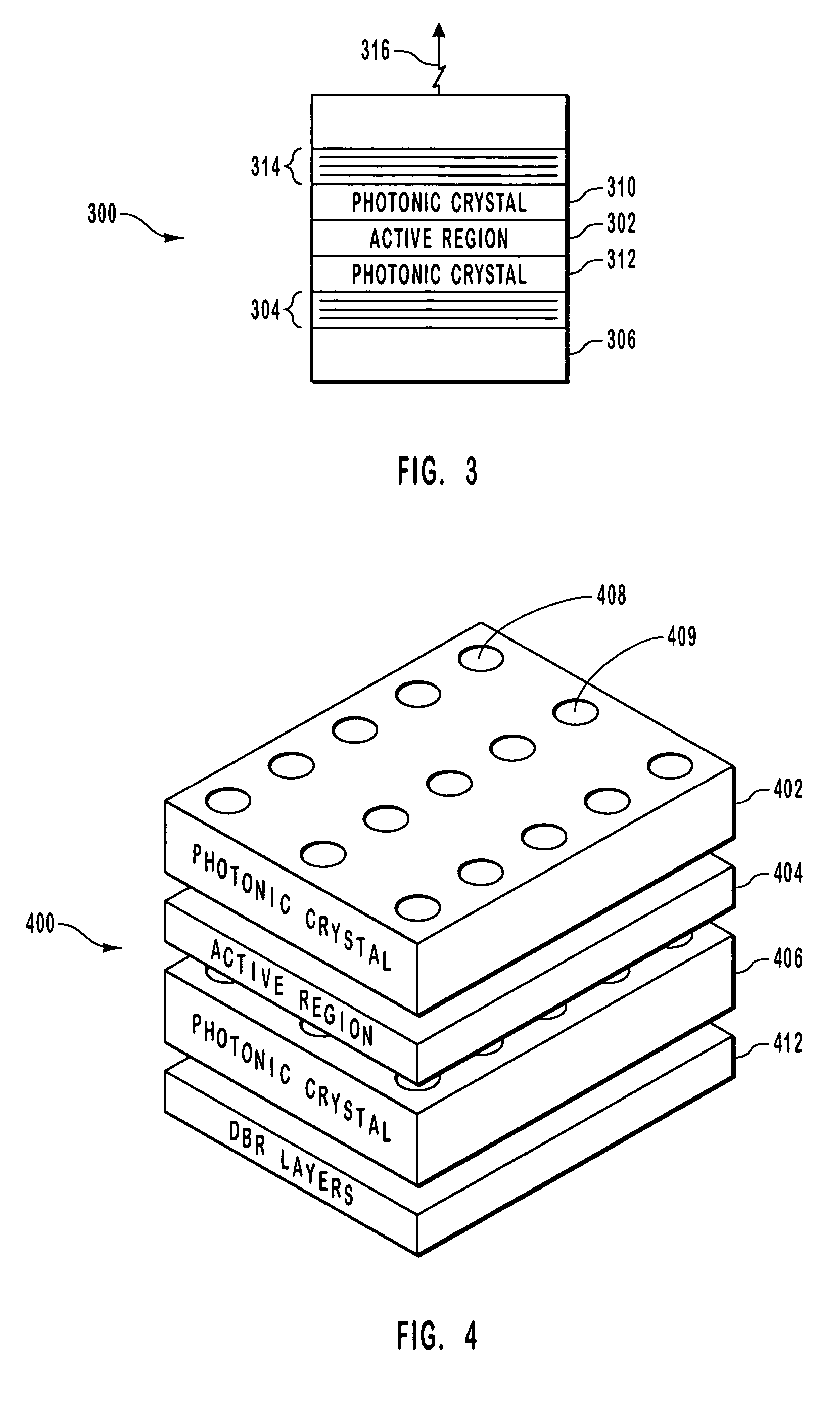
[0022] An 850 nm VCSEL is typically constructed on a semiconductor wafer such as Gallium Arsenide (GaAs). The VCSEL includes a bottom mirror constructed on the semiconductor wafer. Typically, the bottom mirror includes a number of alternating high and low index of refraction layers. As light passes from a layer of one index of refraction to another, a portion of the light is reflected. By using a sufficient number of alternating layers, a high percentage of light can be reflected by the mirror.

[0023] An active region that includes a number of quantum wells is formed on the bottom mirror. The active region forms a PN junction sandwiched between the bottom mirror and a top mirror, which are often of opposite conductivity types (i.e. a p-type mirror and an n-type mirror). Free carriers in the form of holes and electrons are injected into the quantum wells when the PN junction is forward biased by an electrical current. At a sufficiently high bias current (i.e. the threshold current) t...


PUM


Abstract

An optical device including a polarization control photonic crystal. The optical device includes a vertical cavity surface emitting laser. The optical device further includes a lower mirror formed on a substrate. The optical device also includes an upper mirror. An active region is between the lower mirror and the upper mirror. Photons generated in the active region are reflected between the upper mirror and the lower mirror through the active region. An asymmetrical photonic crystal including cavities is optically coupled in the optical device such that one polarization of light is better reflected by the asymmetrical photonic crystal than a competing polarization of light.

Description

BACKGROUND [0001] 1. The Field of the Invention [0002] The invention generally relates to polarization control in VCSELS. More specifically, the invention relates to using photonic crystals to control polarization in VCSELs. [0003] 2. Description of the Related Art [0004] Some of the most commonly used light sources in optical communication systems are semiconductor lasers. Vertical cavity surface emitting lasers (VCSELs) are an example of semiconductor lasers and are used in optical communication systems for several reasons. VCSELs can be manufactured in large quantities due to their relatively small size and can often be tested at the wafer level. VCSELs typically have low threshold currents and can be modulated at high speeds. VCSELs also couple well with optical fibers. [0005] A VCSEL typically requires a high reflectivity mirror system because in a VCSEL, the light resonates in a direction that is perpendicular to the pn-junction. The cavity or active region of a VCSEL is thus ...

Claims


Application Information

Patent Timeline
Patent Type & Authority Applications(United States)
IPC IPC(8): H01S5/00H01S3/08
CPCH01S5/18355H01S5/105H01S5/11H01S5/183
Inventor DENG, HONGYU
Owner II VI DELAWARE INC
Why Eureka
Try Eureka