Semiconductor device

a technology of semiconductors and devices, applied in the direction of semiconductor devices, basic electric elements, electrical appliances, etc., can solve the problems of short channel effect, poor connection, and major defect generation in manufacturing process, and achieve low power consumption, high speed operation, and cost reduction

Active Publication Date: 2011-07-28
SEMICON ENERGY LAB CO LTD
View PDF99 Cites 58 Cited by
  • Summary
  • Abstract
  • Description
  • Claims
  • Application Information

AI Technical Summary

Benefits of technology

[0017]In order to achieve high-speed operation, low power consumption, cost reduction, or the like of a transistor, it is necessary to miniaturize a transistor.
[0019]In addition, in the case where a transistor is miniaturized, a problem of a short-channel effect is also caused. The short-channel effect refers to degradation of electrical characteristics which becomes obvious with miniaturization of a transistor (a reduction in channel length (L)). The short-channel effect results from the effect of an electric field of a drain electrode on a source electrode. Specific examples of the short-channel effect are a decrease in threshold voltage, an increase in subthreshold swing (S value), an increase in leakage current, and the like. In particular, it is known that a transistor including an oxide semiconductor has smaller off current at a room temperature as compared to a transistor including silicon. This is attributed to the fact that carriers generated by thermal excitation are small, that is, carrier density is small. In the transistor in which a material whose carrier density is small is used as described above, a short-channel effect such as a decrease in a threshold voltage tends to be caused easily.
[0035]According to one embodiment of the disclosed invention, either of the following effects or both of the effects can be obtained.
[0036]First, each of the source electrode and the drain electrode is formed to have a stacked structure including the first conductive layer and the second conductive layer, a region which extends in the channel length direction from an end portion of the first conductive layer is provided; thus, coverage in forming a semiconductor layer over the source electrode and the drain electrode is improved. Therefore, occurrence of poor connections or the like can be prevented.
[0037]Second, in the source electrode or the drain electrode, a vicinity of the region in contact with the channel formation region can be high-resistance region, whereby an electric field between the source electrode and the drain electrode can be relieved. Thus, the short-channel effect such as a decrease in a threshold voltage can be suppressed.
[0038]With such an effect, a problem accompanied with miniaturization can be resolved. As a result, the size of a transistor can be sufficiently reduced. By sufficiently reducing the size of the transistor, an area of a semiconductor device including the transistor is decreased, and the number of semiconductor devices obtained from one substrate is increased. Accordingly, manufacturing costs of the semiconductor device can be reduced. Further, since the semiconductor device is downsized, the semiconductor device which is substantially the same in size with further increased function can be realized. Furthermore, effects of high-speed operation, low power consumption, and the like of a transistor can be obtained in accordance with a reduction in channel length. Thus, miniaturization of a transistor including an oxide semiconductor can be achieved according to an embodiment of the disclosed invention, and various effects accompanied with the miniaturization can be obtained.

Problems solved by technology

In the case where a transistor is miniaturized, defects generated in a manufacturing process become a major problem.
For example, each of a source electrode and a drain electrode and a channel formation region are electrically connected; however, disconnections, poor connections, and the like may occur due to a decrease in coverage by the miniaturization.
In addition, in the case where a transistor is miniaturized, a problem of a short-channel effect is also caused.

Method used


Image

  • Semiconductor device
  • Semiconductor device
  • Semiconductor device

Examples


embodiment 1

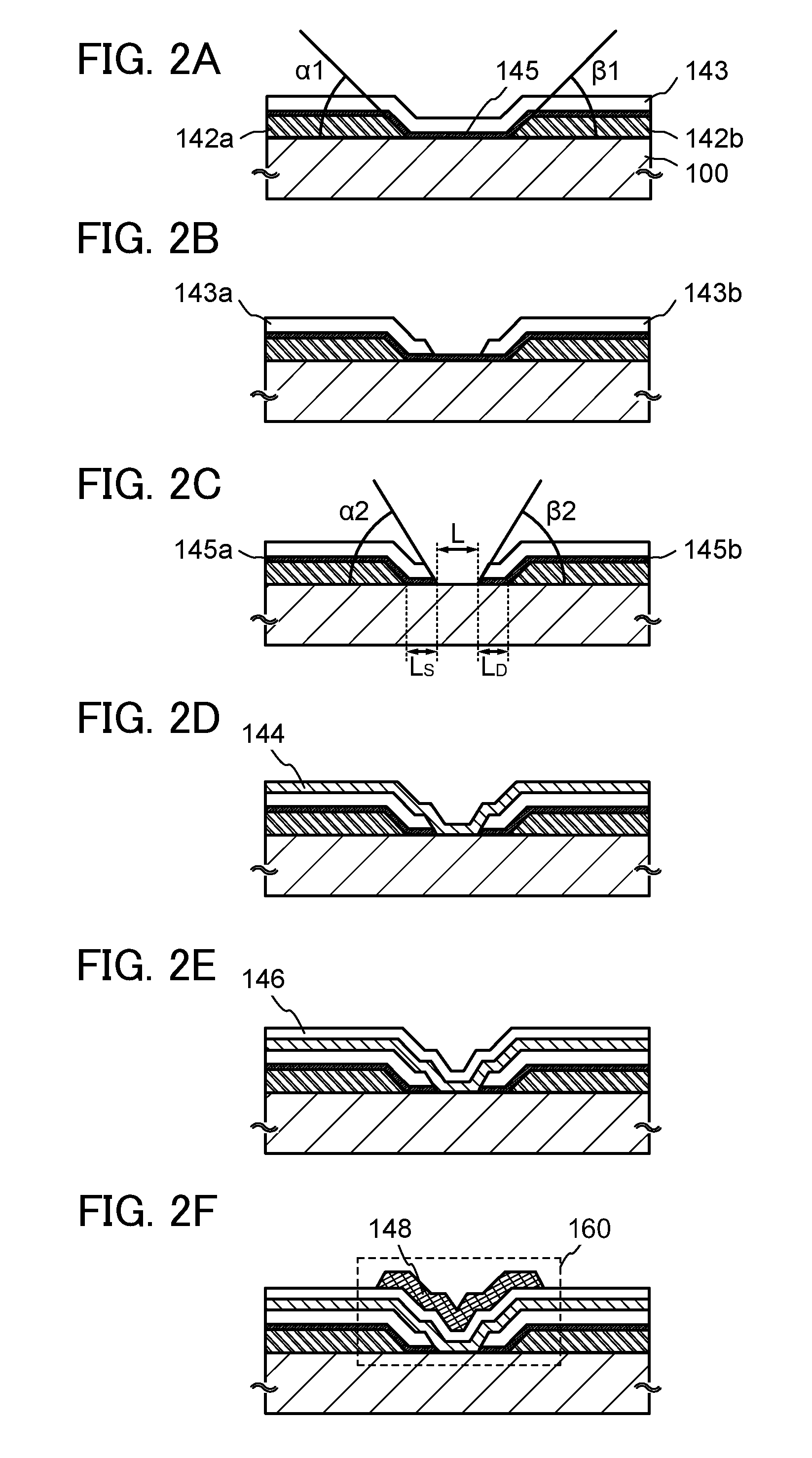
[0057]In this embodiment, an example of a structure and a manufacturing process of a semiconductor device according to an embodiment of the disclosed invention will be described with reference to FIGS. 1A to 1D, FIGS. 2A to 2F, and FIGS. 3A to 3F.

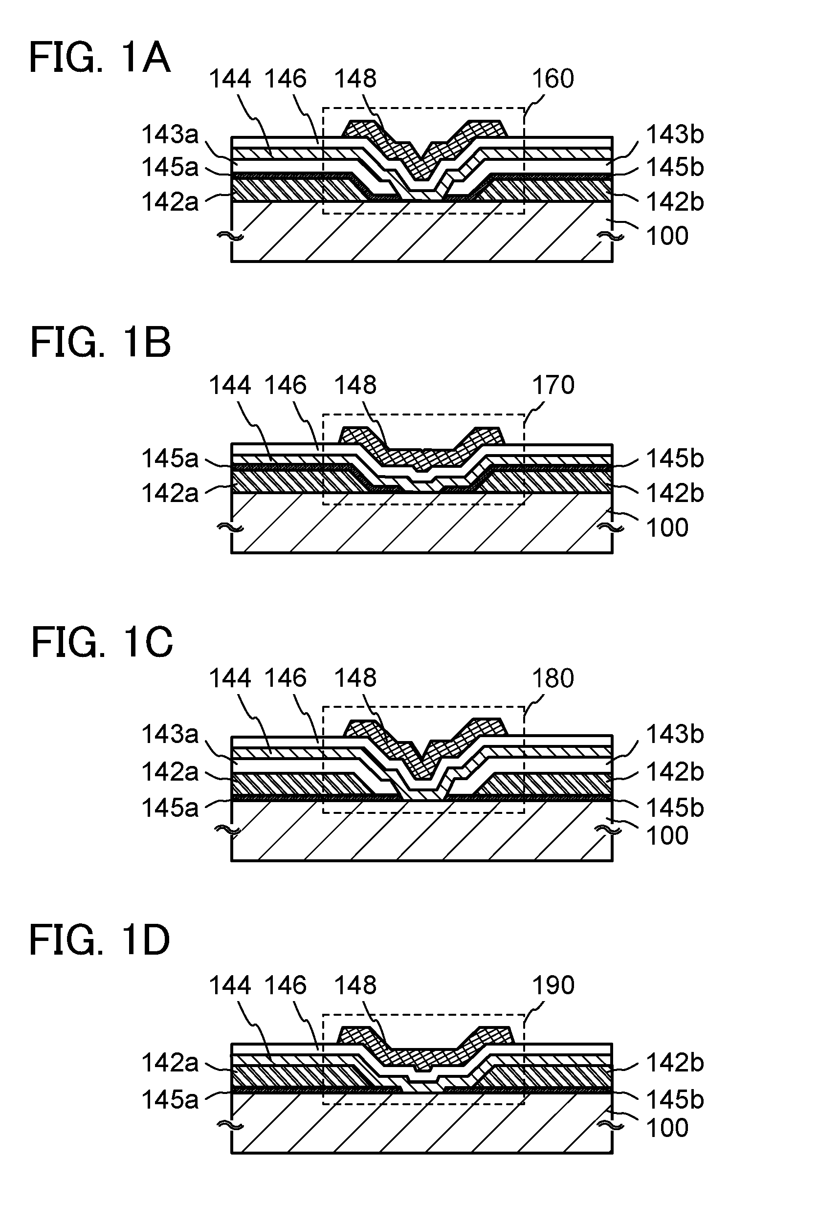
[0058]In FIGS. 1A to 1D, as examples of semiconductor devices, cross-sectional structures of transistors are illustrated. In FIGS. 1A to 1D, top-gate transistors are illustrated as transistors according to one embodiment of the disclosed invention.

[0059]A transistor 160 illustrated in FIG. 1A includes, over a substrate 100, a source electrode in which a first conductive layer 142a and a second conductive layer 145a are stacked in this order; a drain electrode in which a first conductive layer 142b and a second conductive layer 145b are stacked in this order; an insulating layer 143a provided over the source electrode; an insulating layer 143b provided over the drain electrode; an oxide semiconductor layer 144 provided over the insulating la...

embodiment 2

[0129]In this embodiment, a structure and a manufacturing process of a semiconductor device according to one embodiment of the disclosed invention, which are different from those of Embodiment 1, will be described with reference to FIG. 4 and FIGS. 5A to 5F.

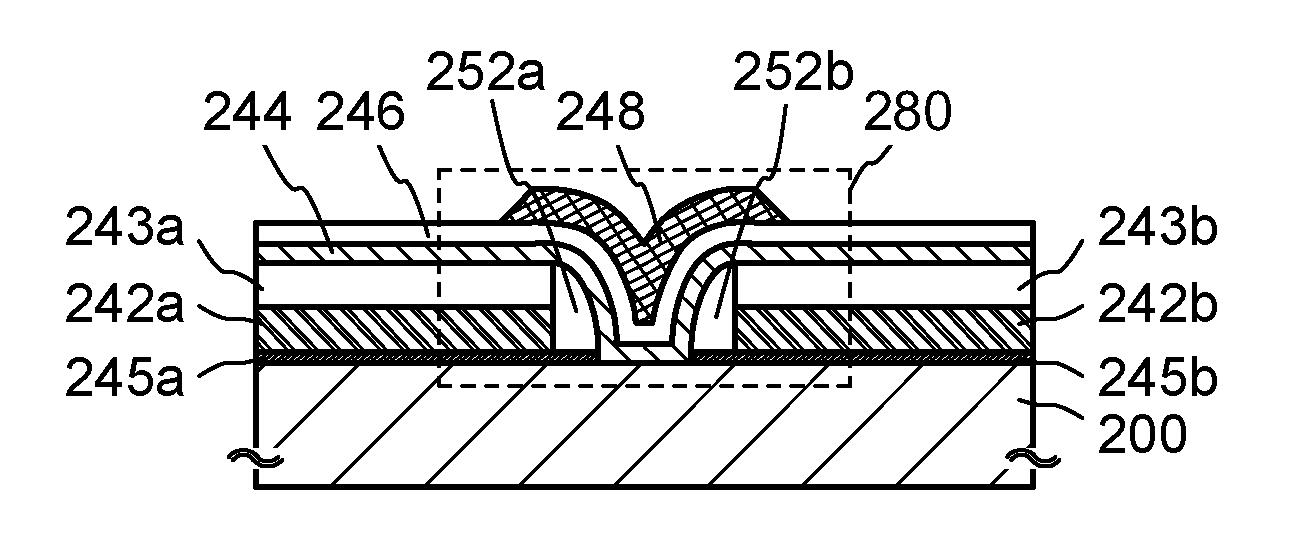
[0130]A transistor 280 illustrated in FIG. 4 is an example of a structure of a semiconductor device. The order of stacking of the transistor 280 corresponds to that of the transistor 180 illustrated in FIG. 1C. The difference between the transistor 280 and the transistor 180 is that a sidewall insulating layer 252a is provided over the second conductive layer 245a in a region which extends in a channel length direction from an end portion of the first conductive layer 242a and a sidewall insulating layer 252b is provided over the second conductive layer 245b in a region which extends in a channel length direction from an end portion of the first conductive layer 242b.

[0131]The transistor 280 illustrated in FIG. 4 includes, over ...

embodiment 3

[0159]In this embodiment, application examples of a semiconductor device according to one embodiment of the disclosed invention will be described with reference to FIGS. 6A-1, 6A-2, and 6B. Here, an example of a memory device will be described. Note that in a circuit diagram, “OS” is written in order to indicate that a transistor includes an oxide semiconductor.

[0160]In the semiconductor device illustrated in FIG. 6A-1, a first wiring (a 1st line) is electrically connected to a source electrode of a transistor 300. A second wiring (a 2nd line) is electrically connected to a drain electrode of the transistor 300. Further, a third wiring (a 3rd line) is electrically connected to one of a source electrode and a drain electrode of a transistor 310, and a fourth wiring (4th Line) is electrically connected to a gate electrode of the transistor 310. A gate electrode of the transistor 300 and the other of the source electrode and the drain electrode of the transistor 310 are electrically co...


PUM


Abstract

An object is to provide a semiconductor device including an oxide semiconductor, which maintains favorable characteristics and achieves miniaturization. The semiconductor device includes an oxide semiconductor layer, a source electrode and a drain electrode in contact with the oxide semiconductor layer, a gate electrode overlapping with the oxide semiconductor layer, and a gate insulating layer provided between the oxide semiconductor layer and the gate electrode, in which the source electrode and the drain electrode each include a first conductive layer, and a second conductive layer having a region which extends in a channel length direction from an end portion of the first conductive layer.

Description

TECHNICAL FIELD[0001]A technical field of the present invention relates to a semiconductor device. Note that semiconductor devices herein refer to general elements and devices which function by utilizing semiconductor characteristics.BACKGROUND ART[0002]There are a wide variety of metal oxides and such metal oxides are used for various applications. Indium oxide is a well-known material and has been used for transparent electrodes required in liquid crystal display devices or the like.[0003]Some metal oxides have semiconductor characteristics. The examples of such metal oxides having semiconductor characteristics are, for example, tungsten oxide, tin oxide, indium oxide, zinc oxide, and the like. A thin film transistor in which a channel formation region is formed using such metal oxides is already known (for example, see Patent Documents 1 to 4, Non-Patent Document 1, and the like).[0004]As metal oxides, not only single-component oxides but also multi-component oxides are known. Fo...

Claims


Application Information

Patent Timeline
Patent Type & Authority Applications(United States)
IPC IPC(8): H01L29/24
CPCH01L29/7869H01L29/41733H01L29/45
Inventor YAMAZAKI, SHUNPEIGODO, HIROMICHISUZAWA, HIDEOMISASAGAWA, SHINYAKURATA, MOTOMUMIKAMI, MAYUMI
Owner SEMICON ENERGY LAB CO LTD
Why Eureka
Try Eureka