Shift register circuit and image display apparatus containing the same

a technology of shift register and image display apparatus, which is applied in logic circuits, digital storage, instruments, etc., can solve the problems of slow output signal rise speed, difficulty in speeding up the operation of each unit shift register, and increase the area of the circuit, so as to speed up the charging of the gate electrode and high-speed operation of the shift register

Active Publication Date: 2008-04-03
TRIVALE TECH LLC
View PDF11 Cites 95 Cited by
  • Summary
  • Abstract
  • Description
  • Claims
  • Application Information

AI Technical Summary

Benefits of technology

[0013]An object of the present invention is to speed up the charging of a gate electrode of an output pull-up transistor in a shift register for use as a gate line driving circuit or the like, thereby allowing a high-speed operation of the shift register.

Problems solved by technology

One method for this is to increase the channel width of the output pull-up transistor, which however involves the problem of increased area of the circuit.
However, in a shift register when used as a gate line driving circuit, output terminals of unit shift registers are connected to gate lines which can be large capacitive loads, so that the rising speeds of the output signals become slow.
This slows down the speed of charging of the gate electrode of the output pull-up transistor in each unit shift register, resulting in difficulty in speeding up the operation of each unit shift register and thus difficulty in speeding up the operation of the gate line driving circuit.
That is, as charging proceeds, the gate-source voltage of the charger transistor decreases and the speed of charging slows down with decreasing drive capability.

Method used


Image

  • Shift register circuit and image display apparatus containing the same
  • Shift register circuit and image display apparatus containing the same
  • Shift register circuit and image display apparatus containing the same

Examples


first preferred embodiment

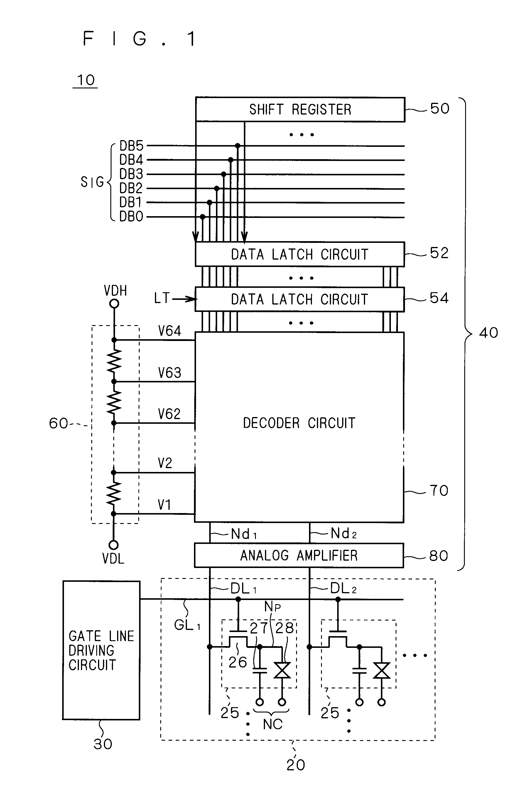
[0038]FIG. 1 is a schematic block diagram showing a configuration of a display apparatus according to a first preferred embodiment of the present invention. It shows an overall configuration of a liquid crystal display 10 as a representative example of the display apparatus.

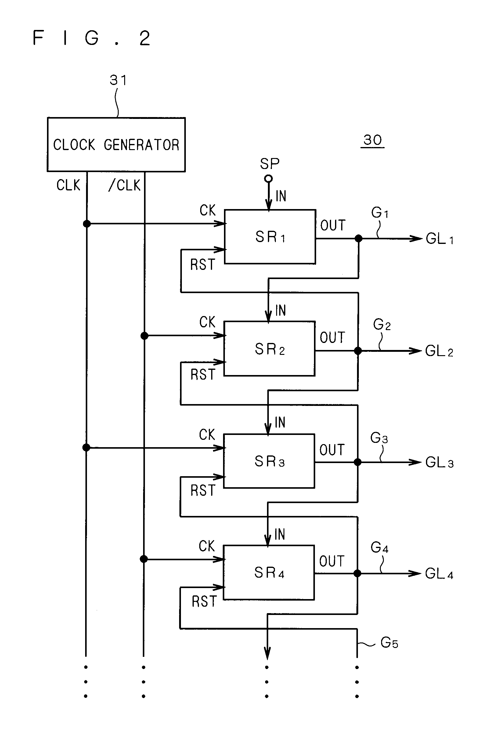
[0039]The liquid crystal display 10 includes a liquid crystal array 20, a gate line driving circuit (scanning line driving circuit) 30, and a source driver 40. As will be clear from the following description, a shift register according to preferred embodiments of the present invention is mounted in the gate line driving circuit 30.

[0040]The liquid crystal array 20 includes a plurality of pixels 25 arranged in a matrix. Gate lines GL1, GL2, . . . (hereinafter also referred to generically as “gate lines GL”) each are provided for each row of pixels (hereinafter also referred to as a “pixel line”), and data lines DL1, DL2, . . . (hereinafter also referred to generically as “data lines DL”) each are provided for each...

second preferred embodiment

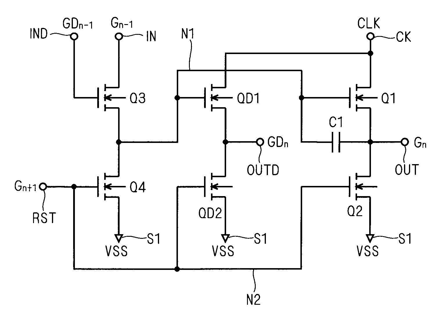
[0116]FIG. 10 is a circuit diagram showing a configuration of a unit shift register SR according to a second preferred embodiment of the present invention. In this figure, elements having similar functions to those shown in FIG. 5 are designated by the same reference numerals or characters.

[0117]While the unit shift registers SR (FIG. 5) according to the first preferred embodiment each have one clock terminal CK, the unit shift registers SR according to the second preferred embodiment each have two clock terminals CK1 and CK2 as shown in FIG. 10. Hereinafter, the clock terminal CK1 is referred to as a “first clock terminal,” and the clock terminal CK2 as a “second clock terminal.”

[0118]The first clock terminal CK1 is equivalent to the clock terminal CK of the unit shift register SR shown in FIG. 5. That is, in this preferred embodiment, a clock signal inputted to the first clock terminal CK1 is supplied to the first and second output terminals OUT and OUTD through the transistors Q1...

third preferred embodiment

[0123]As field-effect transistors included in a gate line driving circuit in a display apparatus, amorphous silicon thin film transistors (a-Si TFTs) are widely used. It is known that a-Si TFTs have threshold voltages that shift largely when their gate electrodes are continuously biased. This phenomenon raises a problem of causing a malfunction in the gate line driving circuit. It is also known that not only a-Si TFTs but also organic TFTs cause a similar problem.

[0124]In the unit shift register SR according to the second preferred embodiment (FIG. 10), for example, the gates of the transistors Q2 and Q2D are repeatedly biased to the HIGH level by a clock signal inputted to the second clock terminal CK2. For this reason, in the case or the unit shift register SR constituted by a-Si TFTs or organic TFTs, the threshold voltages of the transistors Q2 and Q2D shift in the normal direction. This deteriorates the drive capabilities of the transistors Q2 and Q2D and makes it difficult to s...


PUM


Abstract

A high-speed shift register circuit is provided. The shift register circuit includes a first transistor supplying a clock signal to a first output terminal, a second transistor discharging the first output terminal, a third transistor supplying the above clock signal to a second output terminal, and a fourth transistor discharging the second output terminal. The gates of the first and third transistors are both connected to a first node, and the gates of the second and fourth transistors are both connected to a second node. The first node is charged by a fifth transistor which is connected between the first node and a first input terminal and which has a gate connected to a second input end.

Description

BACKGROUND OF THE INVENTION[0001]1. Field of the Invention[0002]The present invention relates to a shift register circuit, and more particularly to a shift register circuit for use as a scanning line driving circuit in an image display apparatus or the like and constituted by only field-effect transistors of the same conductivity type.[0003]2. Description of the Background Art[0004]In an image display apparatus (hereinafter referred to as a “display apparatus”) such as a liquid crystal display, a plurality of pixels are arranged in a matrix in a display panel and a gate line (scanning line) is provided for each row of pixels (pixel line) of the display panel. In a cycle of one horizontal period of a display signal, the gate lines are sequentially selected and driven to update a display image. As a gate line driving circuit (scanning line driving circuit) for sequentially selecting and driving pixel lines, i.e., gate lines, a multi-stage shift register may be used, which performs a r...

Claims


Application Information

Patent Timeline
Patent Type & Authority Applications(United States)
IPC IPC(8): G11C19/28
CPCG11C19/28G09G3/20G11C19/00G09G3/36H03K19/00
Inventor TOBITA, YOUICHI
Owner TRIVALE TECH LLC
Why Eureka
Try Eureka