Drive circuit for display device

Inactive Publication Date: 2002-02-05
SEMICON ENERGY LAB CO LTD
View PDF11 Cites 98 Cited by
  • Summary
  • Abstract
  • Description
  • Claims
  • Application Information

AI Technical Summary

Benefits of technology

It is an object of the present invention to provide a display device driver circuit which is free of the foregoin

Problems solved by technology

At this time, if a constant voltage is kept applied to the liquid crystal material, then it will deteriorate.
However with the prior art display device driver circuit using shift register circuits, if any one of the shift register circuits connected in series is defective, then no signal is transmitted to the following stages of shift register circuits.
This causes a decrease in the production yield of the whole display device.
As a result, the electric power consumed is increased.
Electric charge, however, leaks from this analog memory.
Therefore, it may not be possible to store a required amount of electric charge.
This shortens the life of the display data signal.
As a r

Method used


Image

  • Drive circuit for display device
  • Drive circuit for display device
  • Drive circuit for display device

Examples


Embodiment Construction

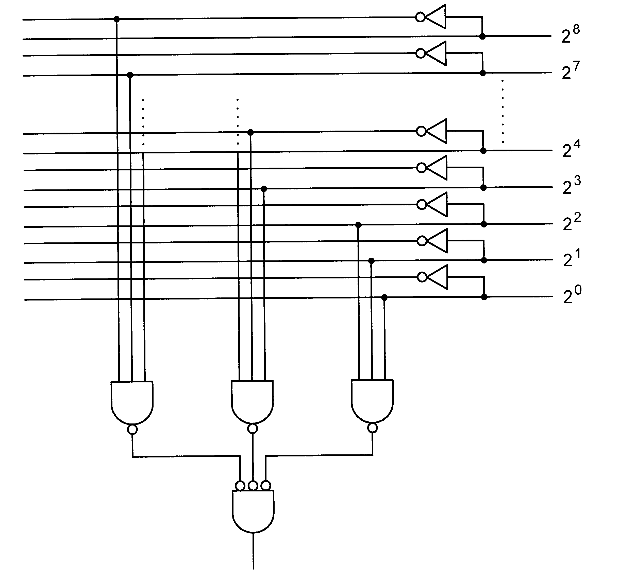
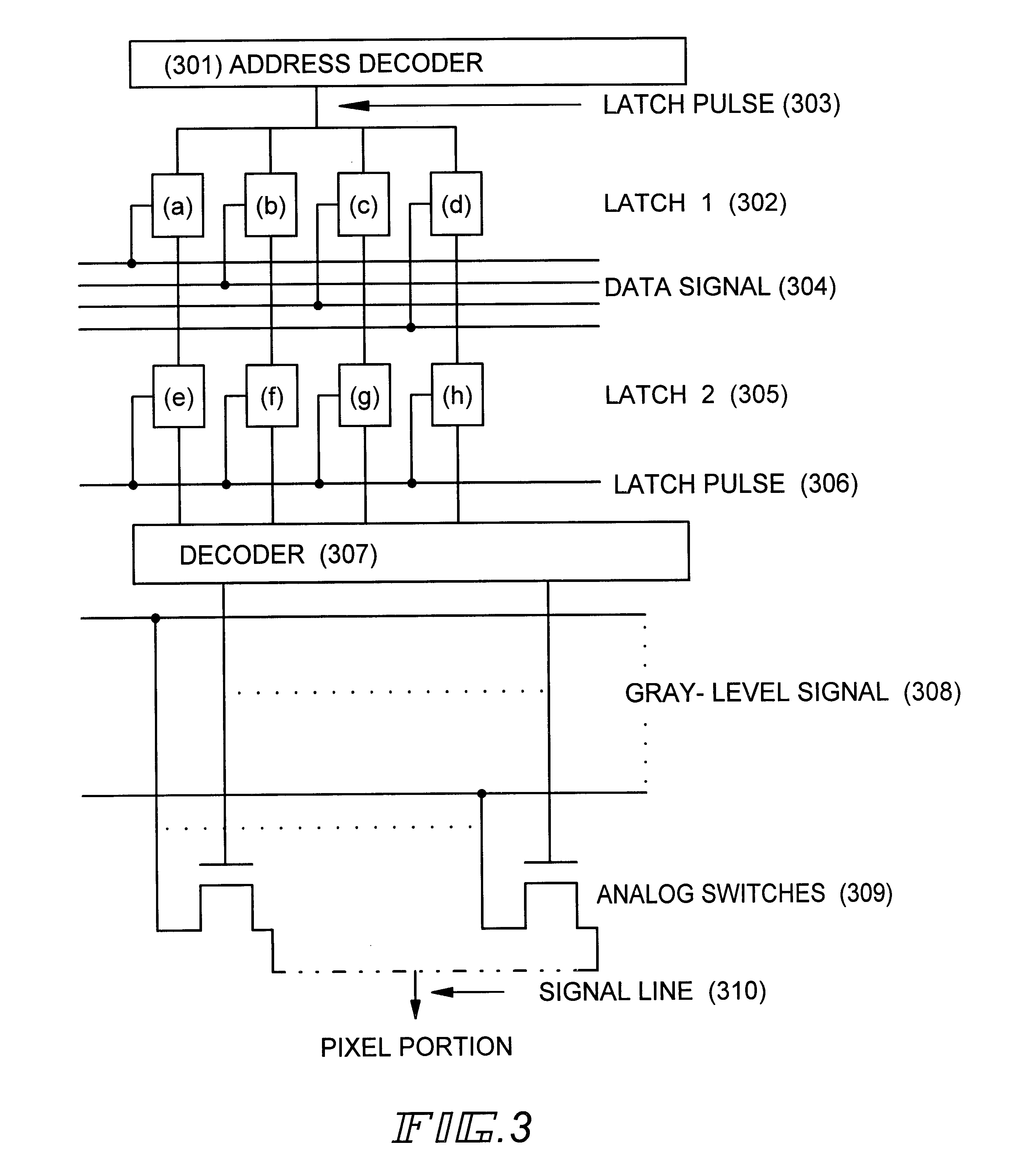
The preferred embodiments of the present invention are hereinafter described. FIG. 3 is a block diagram of a part of a signal line driver circuit which is associated with one signal line. This driver circuit uses an address decoder and has 500 signal lines in this example.

Address signals for pixels to be displayed are applied to the address decoder, 301, via external terminals (not shown). Signal lines are selected according to the values of the address signals. These address signals act as latch pulses for latches 1 (302) which are connected in parallel. The number of the latches 1 is equal to the number of bits of data signal 304 which carries data about gray levels. Each latch 1 (302) consists of a D flip-flop circuit.

The data signal 304 which carries data about gray levels is applied to these latches 1 (302). The latches 1 (302) accept gray-level signals carried by the data signal 304 at the timing of the latch pulses 303 delivered from the address decoder 301. The results are s...


PUM


Abstract

A driver circuit for use in an active matrix display having switching devices at pixels. The driver circuit uses no shift registers. Random access to signal lines or scanning lines can be obtained. The display quality is improved. The production yield is improved. Also, lower electric power consumption and higher-speed operation can be accomplished. Data about gray levels assumes the form of digital values and is supplied to the driver circuit. The signal lines or scanning lines are selected by an address decoder circuit.

Description

BACKGROUND OF THE INVENTION1. Field of the InventionThe present invention relates to a driver circuit for use in a display device and, more particularly, to a driver circuit adapted for use in an active matrix liquid crystal display.2. Description of the Prior ArtHeretofore, a driver circuit for use in a display device such as an active matrix liquid crystal display adopted line-sequential scanning making use of shift registers.The prior art liquid crystal display is schematically shown in FIG. 1. A signal line driver circuit 101 and a scanning line driver circuit 102 are formed on the same glass substrate. Also, a liquid crystal pixel portion 103 is created in the center of the display device.The driver circuits 101 and 102 are connected with the liquid. crystal pixel portion 103 by signal lines X1, X2, . . . extending in the direction of columns and by signal lines Y1, Y2, . . . extending in the direction of rows. Thin-film transistors (TFTs) acting as switching devices are formed...

Claims


Application Information

Patent Timeline
IPC IPC(8): G09G3/36G02F1/133
CPCG09G3/3688G09G2310/027G09G3/36
Inventor KOYAMA, JUNSUZUKI, RITSUKO
Owner SEMICON ENERGY LAB CO LTD
Why Eureka
Try Eureka