Field emission device

a field emission and laser vaporization technology, applied in the manufacture of discharge tubes/lamps, discharge tube main electrodes, electric discharge tubes/lamps, etc., can solve the problems of carbon nanotubes formed by arc discharge and laser vaporization methods that cannot satisfactorily be used as field emission materials, and the height and orientation of carbon nanotubes are not uniform, and the resulting material is not suitable for field emission

Inactive Publication Date: 2004-05-20
TSINGHUA UNIV +1
View PDF4 Cites 60 Cited by
  • Summary
  • Abstract
  • Description
  • Claims
  • Application Information

AI Technical Summary

Benefits of technology

[0009] Another object of the present invention is to provide a field emission device using carbon nanotubes which has a decreased field emission threshold voltage thereof.

Problems solved by technology

Carbon nanotubes formed by any of these methods alone cannot satisfactorily be used as field emission material for the following reasons.
Carbon nanotubes formed using the arc discharge and laser vaporization methods have non-uniform heights and orientations, and are prone to be tangled together.
If the carbon nanotubes are directly used as field emission material, they tend to reduce field concentration and field efficiency.
In addition, cavities at the tips of carbon nanotubes are encapsulated by catalytic metal particles, thereby reducing field concentration and efficiency.
This makes the method unduly time-consuming.
This induces shielding between adjacent carbon nanotubes, reduces field concentration and efficiency, and increases a threshold voltage of field emission.

Method used


Image

  • Field emission device
  • Field emission device
  • Field emission device

Examples


Embodiment Construction

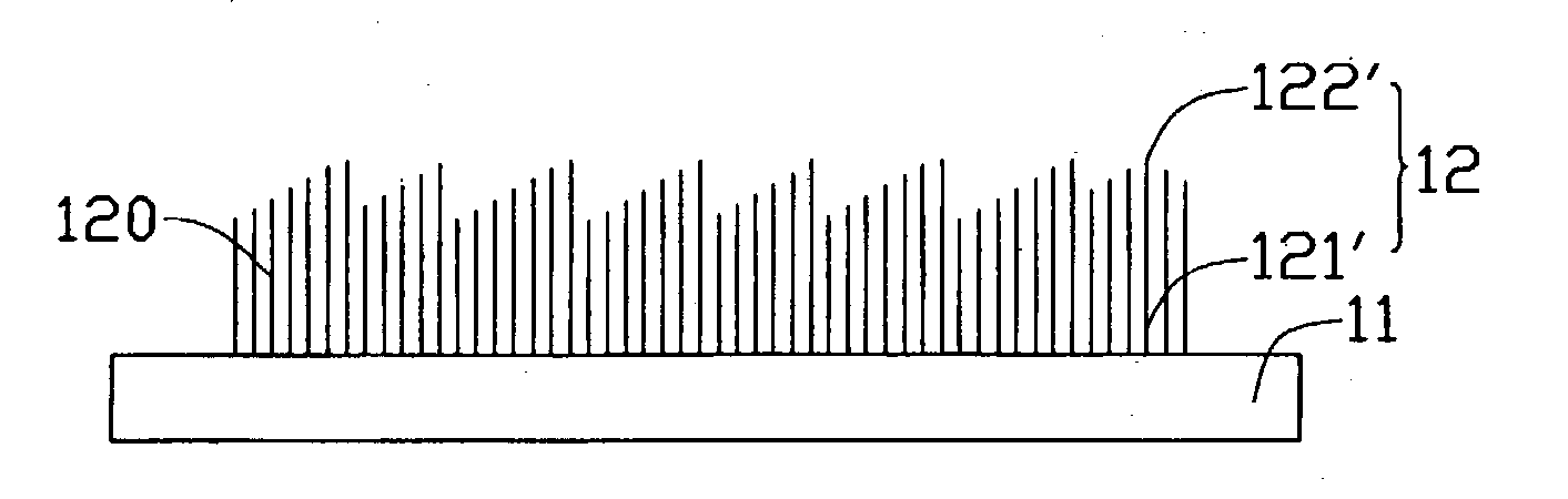
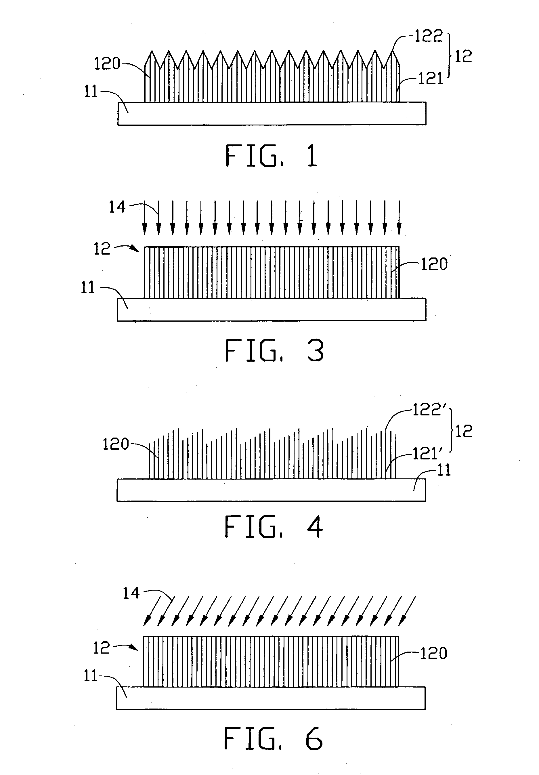
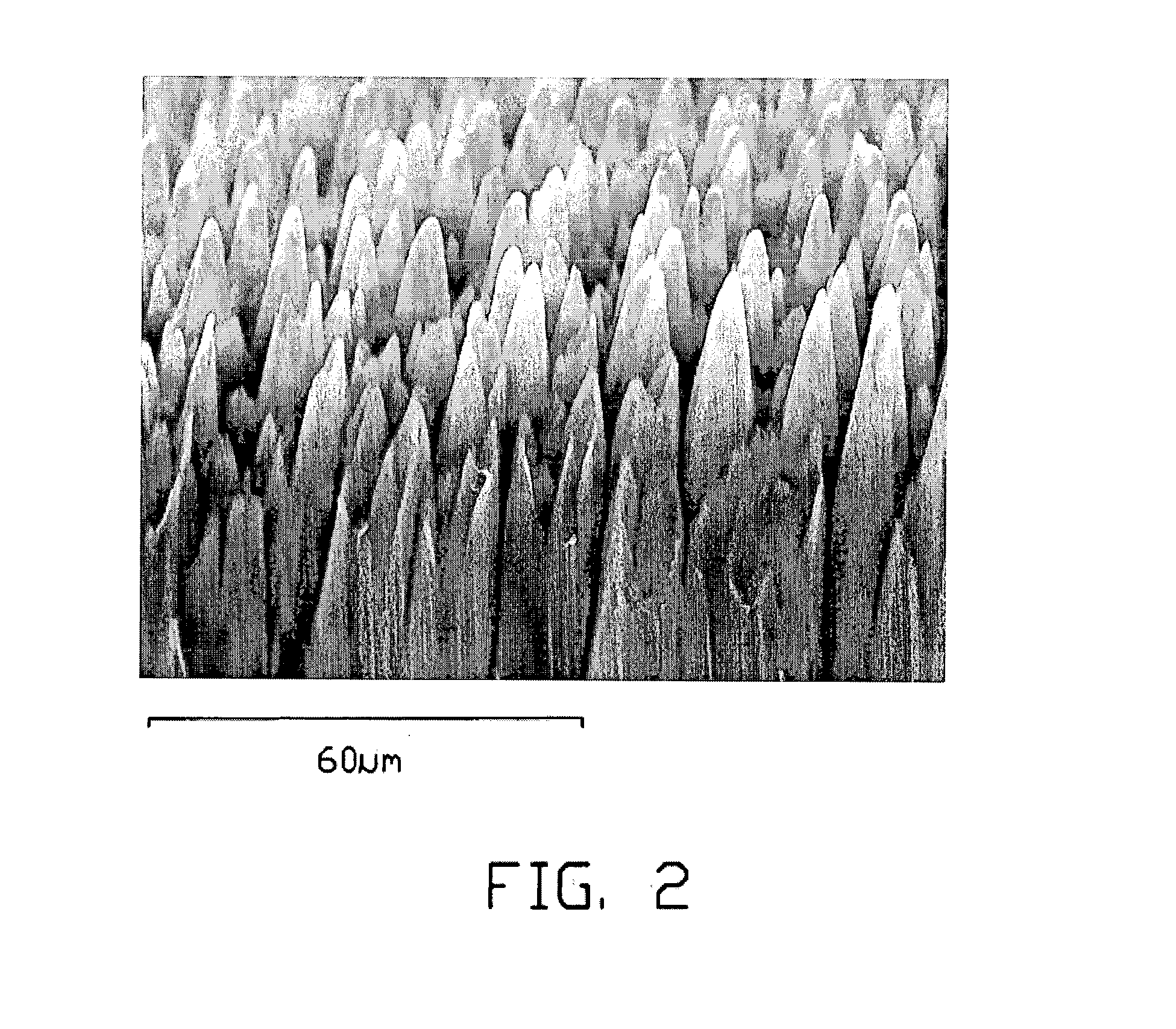
[0020] Referring to FIG. 1, a field emission device in accordance with a preferred embodiment of the present invention comprises a substrate 11 and a carbon nanotube array 12 formed thereon. The substrate 11 can be made of glass, silicon, alumina or another suitable material. The carbon nanotube array 12 can be formed by growing them on the substrate 11 directly, or by transplanting pre-prepared carbon nanotubes onto the substrate 11. Carbon nanotubes 120 of the carbon nanotube array 12 are substantially parallel to each other, and are each substantially perpendicular to the substrate 11. The carbon nanotubes 120 cooperatively form a plurality of lower portions 121 and a plurality of corresponding tapered tips 122 above the lower portions 121. Each lower portion 121 and tapered tips 122 comprise a plurality of carbon nanotubes 120. Each tip 122 is oriented substantially perpendicular to the substrate 11. Distances between adjacent tips 122 are approximately uniform, and are more tha...


PUM

PropertyMeasurementUnit
distanceaaaaaaaaaa
distancesaaaaaaaaaa
diameteraaaaaaaaaa

Abstract

A field emission device includes a substrate (11) and a carbon nanotube array (12) formed thereon. Carbon nanotubes (120) of the carbon nanotube array are parallel to each other and cooperatively form a plurality of substantially rod-shaped lower portions (121, 121') and a plurality of corresponding tapered tips (122, 122') above the lower portions. Each lower portion and tapered tips have a plurality of carbon nanotubes. Distances between adjacent tips are approximately uniform, and are more than one micrometer. Preferably, the distance is in the range from 1 to 30 micrometers. The field emission device with this structure has reduced shielding between adjacent carbon nanotubes and has decreased threshold voltage required for field emission by the carbon nanotubes. The field emission device also contributes to an improved field emission concentration and efficiency.

Description

[0001] 1. Field of the Invention[0002] The present invention relates to a field emission device, and more particularly to a field emission device using carbon nanotubes. The application relates to a contemporaneously filed application having the same applicant and the same assignee with the instant invention, and titled "METHOD FOR PROCESSING ONE-DIMENSIONAL NANO-MATERIALS".[0003] 2. Description of Prior Art[0004] Carbon nanotubes were first discovered and reported in an article by Sumio Iijima entitled "Helical Microtubules of Graphitic Carbon" (Nature, Vol. 354, Nov. 7, 1991, pp. 56-58). Carbon nanotubes have superior electron emission capability at low emission voltages, generally less than 100 volts. Furthermore, carbon nanotubes can carry high electric currents reliably. Due to these properties, carbon nanotubes are considered to be an ideal field emission material for applications in a variety of display devices including flat panel displays, such as field emission displays.[0...

Claims


Application Information

Patent Timeline
Patent Type & Authority Applications(United States)
IPC IPC(8): B82B1/00H01J1/304
CPCB82Y10/00H01J2201/30469H01J1/3044B82Y30/00
Inventor LIU, LIANGFAN, SHOUSHAN
Owner TSINGHUA UNIV
Why Eureka
Try Eureka