Method for fabricating touch sensor panels

A touch sensor, panel technology, applied in printed circuit manufacturing, instruments, dual-use resists, etc., can solve the problems of expensive, high equipment and material costs, achieve effective manufacturing processes, reduce material costs and operating costs, and reduce steps. effect of numbers

Inactive Publication Date: 2012-02-08
APPLE INC
View PDF4 Cites 5 Cited by
  • Summary
  • Abstract
  • Description
  • Claims
  • Application Information

AI Technical Summary

Problems solved by technology

Traditional photolithography/etching processes are

Method used


Image

  • Method for fabricating touch sensor panels
  • Method for fabricating touch sensor panels
  • Method for fabricating touch sensor panels

Examples


Embodiment Construction

[0021] In the following description of the preferred embodiments, reference is made to the accompanying drawings which form a part hereof, and which illustrate specific embodiments that can be practiced. It is to be understood that other embodiments may be utilized and structural changes may be made without departing from the scope of the various embodiments of the present disclosure.

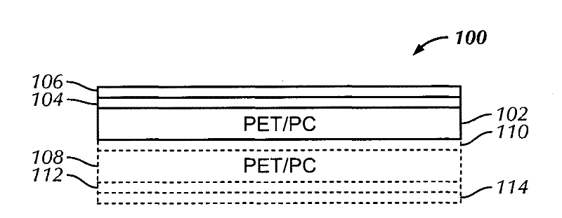
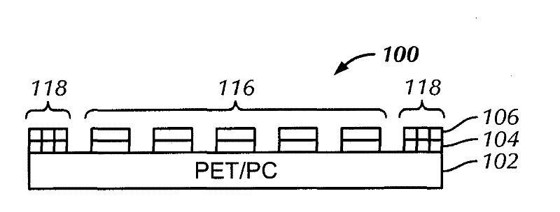
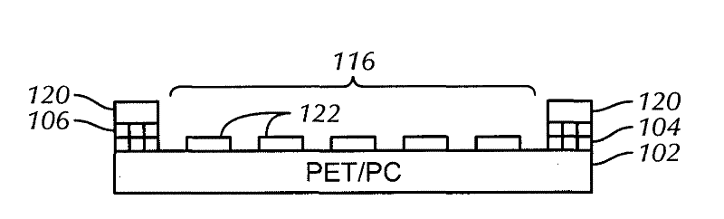
[0022] The invention relates to a method for manufacturing a touch sensor panel. In some touch sensor panel manufacturing processes, photoresist is applied to the panel during the photolithography / etch patterning process. The photoresist is stripped after the photolithography / etch patterning process is complete. A separate passivation layer is then applied in a subsequent passivation treatment. Thus, the entire manufacturing process is tedious and inefficient. Equipment and material costs are also relatively high due to the multiple printing and etching steps performed. Embodiments of the p...


PUM


Abstract

A method for fabricating a touch sensor panel is disclosed. The method includes providing a substrate for the touch sensor panel, depositing a conductive material layer on a top surface of the substrate, depositing a metal layer on top of the conductive material layer, affixing a resist to a first area of the metal layer, the resist also adapted to serve as a passivation layer during passivation, removing metal from the metal layer outside of the first area; and performing passivation on the substrate while leaving the affixed resist intact.

Description

field of invention [0001] The present invention relates generally to the manufacture of touch sensor panels, and more particularly to the improved Systems and methods for a touch sensor panel manufacturing process. Background technique [0002] In recent years, touch sensor panels, touch screens, and the like have become available as input devices. In particular, touch screens are gaining popularity due to their ease of operation and versatility and their reduction in price. A touch screen may include a touch sensor panel, which may be a transparent panel with a touch-sensitive surface, and a display device, which may be an LCD panel and may be located partially or completely behind the touch-sensor panel so that the touch-sensitive surface can cover the Display at least a portion of the visible area of ​​the device. In some devices, the touch screen is protected by a cover glass. A touch screen may allow a user to perform various functions by touching the touch sensor p...

Claims


Application Information

Patent Timeline
IPC IPC(8): G06F3/041
CPCG06F2203/04103H05K3/064H05K2203/0571Y10T156/10G06F3/0446G06F3/0445
Inventor 黄丽丽S·莫哈帕特拉仲正中
Owner APPLE INC
Why Eureka
Try Eureka