Device and method for measuring surface local electronic state of material

A technology of measuring devices and measuring methods, which is applied in the direction of measuring devices, instruments, scanning probe microscopy, etc., and can solve problems such as complex preparation processes

Active Publication Date: 2012-02-15
SUZHOU INST OF NANO TECH & NANO BIONICS CHINESE ACEDEMY OF SCI
View PDF5 Cites 17 Cited by
  • Summary
  • Abstract
  • Description
  • Claims
  • Application Information

AI Technical Summary

Problems solved by technology

However, the sample preparation process of this method is very complicated, and the evaporated oxide layer and electrodes may make the measured surface electronic state information different from that of the bare clean sample surface, and metal electrodes are usually micron to millimeter scale Macroscopic electrodes, which also give the overall average performance of the device

Method used


Image

  • Device and method for measuring surface local electronic state of material
  • Device and method for measuring surface local electronic state of material
  • Device and method for measuring surface local electronic state of material

Examples


Embodiment Construction

[0013] The specific implementation of the device and method for measuring the surface localized electronic state of a material provided by the present invention will be described in detail below with reference to the accompanying drawings.

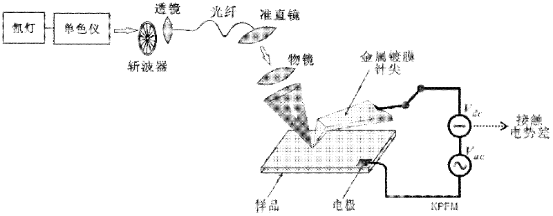
[0014] attached figure 1 Shown is a schematic structural view of the device according to the specific embodiment of the present invention, including: a sample stage, a DC signal generator, an AC signal generator, a wavelength-tunable monochromatic light source, and a metal-coated probe.

[0015] The probe includes a cantilever beam and a needle point arranged at the end of the cantilever beam, the needle point protrudes outward, and the position of the point of the vertical projection of the needle point on the surface of the sample stage is outside the range of the vertical projection plane of the cantilever beam on the surface of the sample stage . This is to avoid the needle tip from blocking the light path, so a probe structure in whi...


PUM


Abstract

The invention discloses a device for measuring the surface local electronic state of a material. The device comprises a sample stage, a direct-current signal generator, an alternating-current signal generator, an adjustable-wavelength monochromatic light source and a metal film-coated probe, wherein the sample stage is conductive; the probe is arranged on the surface of the sample stage, and is kept a certain distance away from the sample stage to accommodate a sample to be measured; one of the two output ends of the direct-current signal generator and the alternating-current signal generator is connected to the sample stage, and the other output end is connected to the probe; light beams emitted by the adjustable-wavelength monochromatic light source are focused light beams; and the focused light beams can be focused onto the needle point of the probe.

Description

technical field [0001] The invention relates to the technical field of semiconductor material testing, in particular to a measuring device and a measuring method for the surface localized electronic state of a material. Background technique [0002] For semiconductor optoelectronic devices, the surface electronic states caused by factors such as dangling bonds, adsorption, defects, impurities and polarity on the surface of materials will have a crucial impact on the photoelectric conversion process. For example, in solar photovoltaic devices, the photogenerated carriers in the PN junction region move in the opposite direction under the action of the built-in electric field, and finally reach the electrode. In this process, the recombination caused by the scattering of carriers by the surface electronic state affects the photovoltaic An important factor of efficiency, regulating the surface state and inhibiting surface recombination is one of the keys to improve photovoltaic ...

Claims


Application Information

Patent Timeline
Patent Type & Authority Applications(China)
IPC IPC(8): G01Q60/24G01Q60/40
Inventor 刘争晖徐耿钊樊英民钟海舰徐科
Owner SUZHOU INST OF NANO TECH & NANO BIONICS CHINESE ACEDEMY OF SCI
Why Eureka
Try Eureka