Device and method for measuring surface defect of semiconductor material

A technology for measuring devices and measuring methods, applied in measuring devices, material excitation analysis, instruments, etc., can solve problems such as low luminous efficiency, difficulty in measuring spectra, low carrier injection energy density, etc., and achieve excellent signal-to-noise ratio, shielding The effect of measuring the impact of the outcome

Inactive Publication Date: 2012-06-13
SUZHOU INST OF NANO TECH & NANO BIONICS CHINESE ACEDEMY OF SCI
View PDF11 Cites 25 Cited by
  • Summary
  • Abstract
  • Description
  • Claims
  • Application Information

AI Technical Summary

Problems solved by technology

However, due to the limitations of the working principle of the scanning tunneling microscope, the tunne

Method used


Image

  • Device and method for measuring surface defect of semiconductor material
  • Device and method for measuring surface defect of semiconductor material
  • Device and method for measuring surface defect of semiconductor material

Examples


Embodiment 1

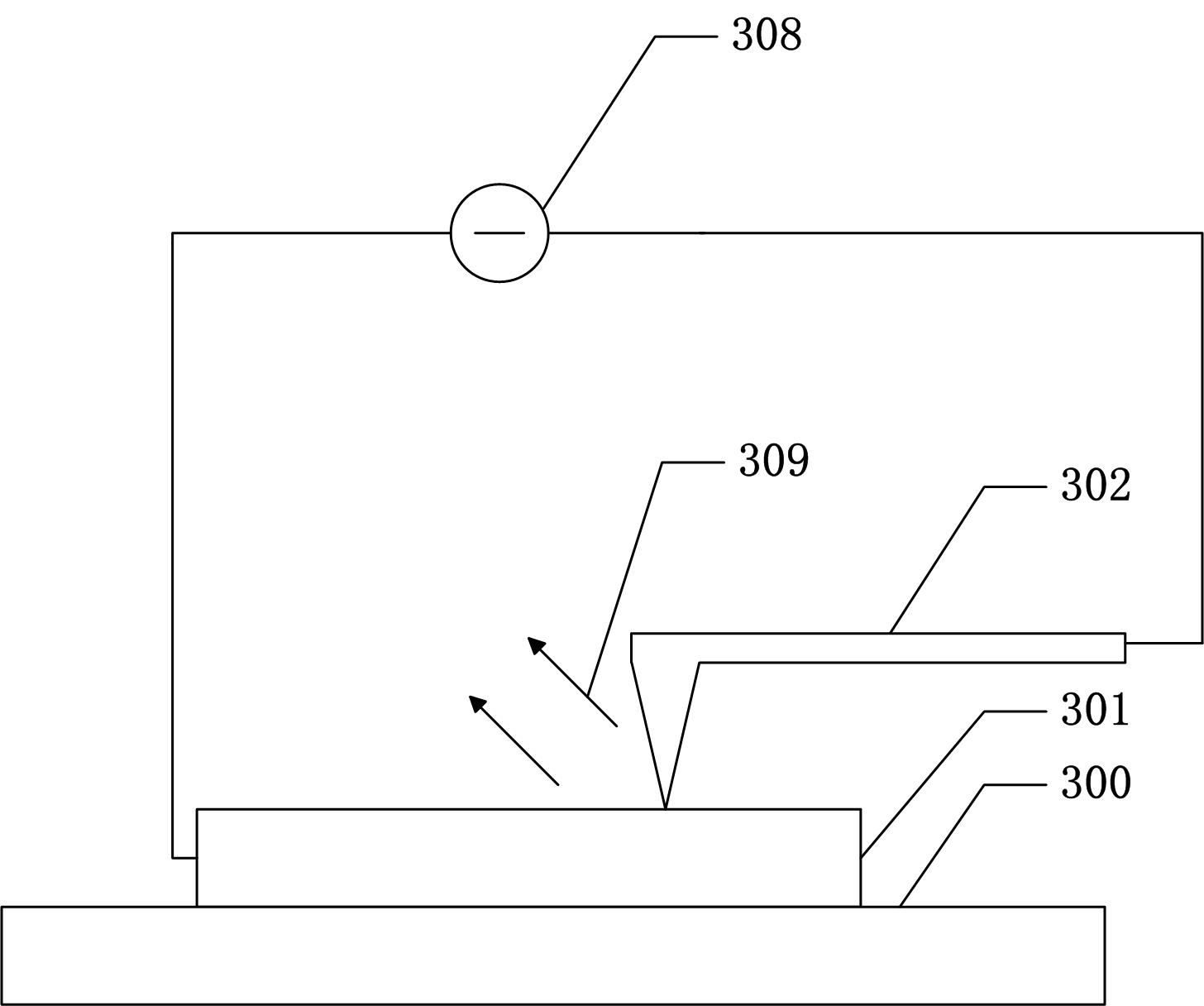
[0038] figure 1Shown is a semiconductor material surface defect measurement device provided by the present invention, including: an atomic force microscope conductive probe 302, the atomic force microscope conductive probe 302 includes a cantilever beam 302b and a tip 302a at the end of the cantilever beam 302b, for Contact with the sample 301 to be tested and inject current into the exposed surface of the sample 301 to be tested; an atomic force microscope control device is mechanically connected with the conductive probe 302 of the atomic force microscope; an optical microscope system 304 is used to collect the surface of the sample 301 to be tested Electroluminescence 309 emitted from the exposed surface; a three-dimensionally movable sample stage 300 for placing the sample 301 to be tested; and a photodetector 306 for detecting the signal of the electroluminescence 309 .

[0039] The measuring device further includes a voltage source 308, one end is electrically connected ...

Embodiment 2

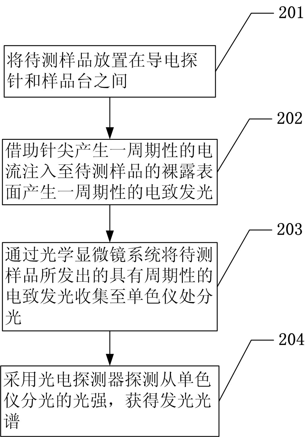
[0046] figure 2 Shown is the flow chart of the second step of the embodiment of the surface defect measurement method provided by the present invention, including: step 201, placing the sample to be tested between the conductive probe of the atomic force microscope and the sample stage; step 202, generating a periodic The current is injected into the exposed surface of the sample to be tested to generate a periodical electroluminescence; step 203, the periodic electroluminescence emitted by the sample to be tested is collected by the optical microscope system to the monochromator for light distribution; step 204, A photodetector is used to detect the light intensity split from the monochromator to obtain a luminescence spectrum.

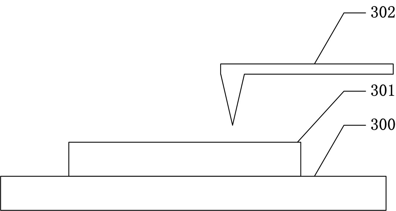
[0047] Figure 3A Shown is step 201 of the second embodiment of the surface defect measurement method provided by the present invention, a sample 301 to be tested is placed between the sample stage 300 and the conductive probe 302 of the atomic for...


PUM


Abstract

The invention provides a device and a method for measuring a surface defect of a semiconductor material, and belongs to the field of semiconductor tests. The device comprises a sample table, an atomic force microscope conductive probe, a voltage source, a piezoelectric exciting ceramic, an optical microscope system, a monochrometer, a photoelectric detector and a phase lock amplifier, wherein the voltage source and the piezoelectric exciting ceramic are connected with the atomic force microscope conductive probe; and the monochrometer, the photoelectric detector and the phase lock amplifier are connected with one another sequentially. The method comprises the following steps of: putting a sample to be measured on the sample table; making the tip of the probe generate a periodic mechanical vibration; generating periodic light on the exposed surface of the sample to be measured; focusing the light emitted by the sample to be measured on the monochrometer for splitting the light; and measuring a luminous signal. According to the device and the method, the problem that electroluminescent spectra exist during measurement of the surface defect of a semiconductor in the prior art is solved; furthermore, the influence of stray light on a measurement result is avoided; and a high signal to noise ratio.

Description

technical field [0001] The invention relates to the technical field of semiconductor material detection, in particular to a semiconductor material surface defect measurement device and a surface defect measurement method. Background technique [0002] For semiconductor optoelectronic devices, various non-radiative recombination centers caused by defect structures in materials are important factors affecting the performance of optoelectronic devices. For example, in gallium nitride materials used as light-emitting diodes, there are usually various dangling bonds and aggregations of dopant atoms at the defect site, thereby forming a defect electronic state, so that carriers are trapped near the defect center and will not produce recombination light emission. . Therefore, measuring these defect states and their effects on carrier recombination emission is very important for device and material research. [0003] Due to defects in materials, especially various line dislocation...

Claims


Application Information

Patent Timeline
IPC IPC(8): G01N21/66G01Q60/24
Inventor 刘争晖徐耿钊钟海舰樊英民曾雄辉周桃飞邱永鑫王建峰徐科
Owner SUZHOU INST OF NANO TECH & NANO BIONICS CHINESE ACEDEMY OF SCI
Why Eureka
Try Eureka