Encapsulation construction for silicon crystal microphone

A technology of microphone and silicon crystal, which is applied in the field of packaging structure of silicon crystal microphone, can solve the problems of bulky packaging structure, unsuitable for industrial use, and impracticality, etc., and achieve the effect of simple packaging process, wide adaptability, and noise reduction

Inactive Publication Date: 2008-12-17
MERRY ELECTRONICS CO LTD
View PDF1 Cites 13 Cited by
  • Summary
  • Abstract
  • Description
  • Claims
  • Application Information

AI Technical Summary

Problems solved by technology

[0003] The above-mentioned existing structure still has many deficiencies in practice. Since there is air in the chamber 5 between the upper cover 2 and the base plate 1 for transmitting sound waves, when the temperature of the external environment changes, for example, it moves from the air-conditioning room to the air-conditioning room. When it is hot outdoors, between the upper cover 2 and the electronic component 6 made of different materials, the temperature in the chamber 5 will generate fine water vapor to condense on the upper cover 2 or the electronic component 6 because the temperature is still kept at a low temperature. Between, it is easy to cause damage to the upper cover 2 and the electronic components 6 due to the influence of moisture
[0004] Also, the upper cover 2 is a cup made of metal. If it is affected by water vapor, the insulation effect between the electronic components 6 and the upper cover 2 is likely to be poor. There will also be the same problem, which will greatly affect the electrical properties and efficacy of the product
[0005] Furthermore, the upper cover 2 has a predetermined fixed configuration in order to form the cavity 5, which also causes the entire package structure to be too bulky. In addition, the packaging method using the upper cover 2 is quite different from the current mature semiconductor packaging method. Large, this kind of design that does not conform to industrial use is very impractical, so there is a need for improvement

Method used


Image

  • Encapsulation construction for silicon crystal microphone
  • Encapsulation construction for silicon crystal microphone
  • Encapsulation construction for silicon crystal microphone

Examples


Embodiment Construction

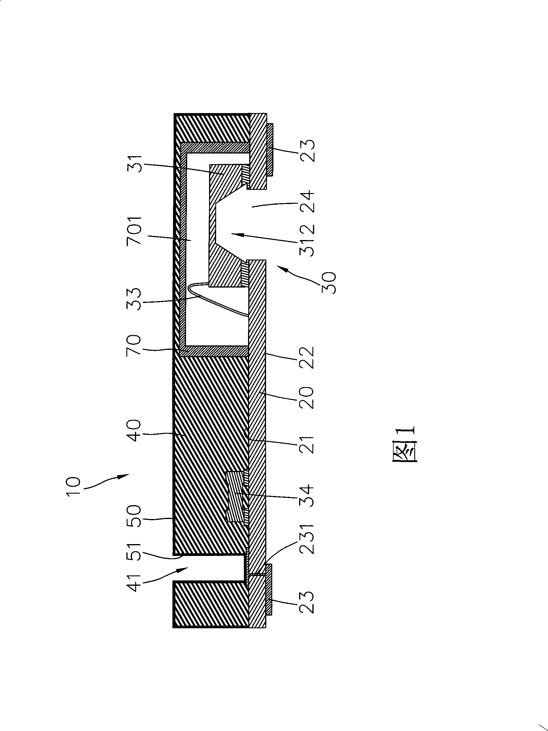
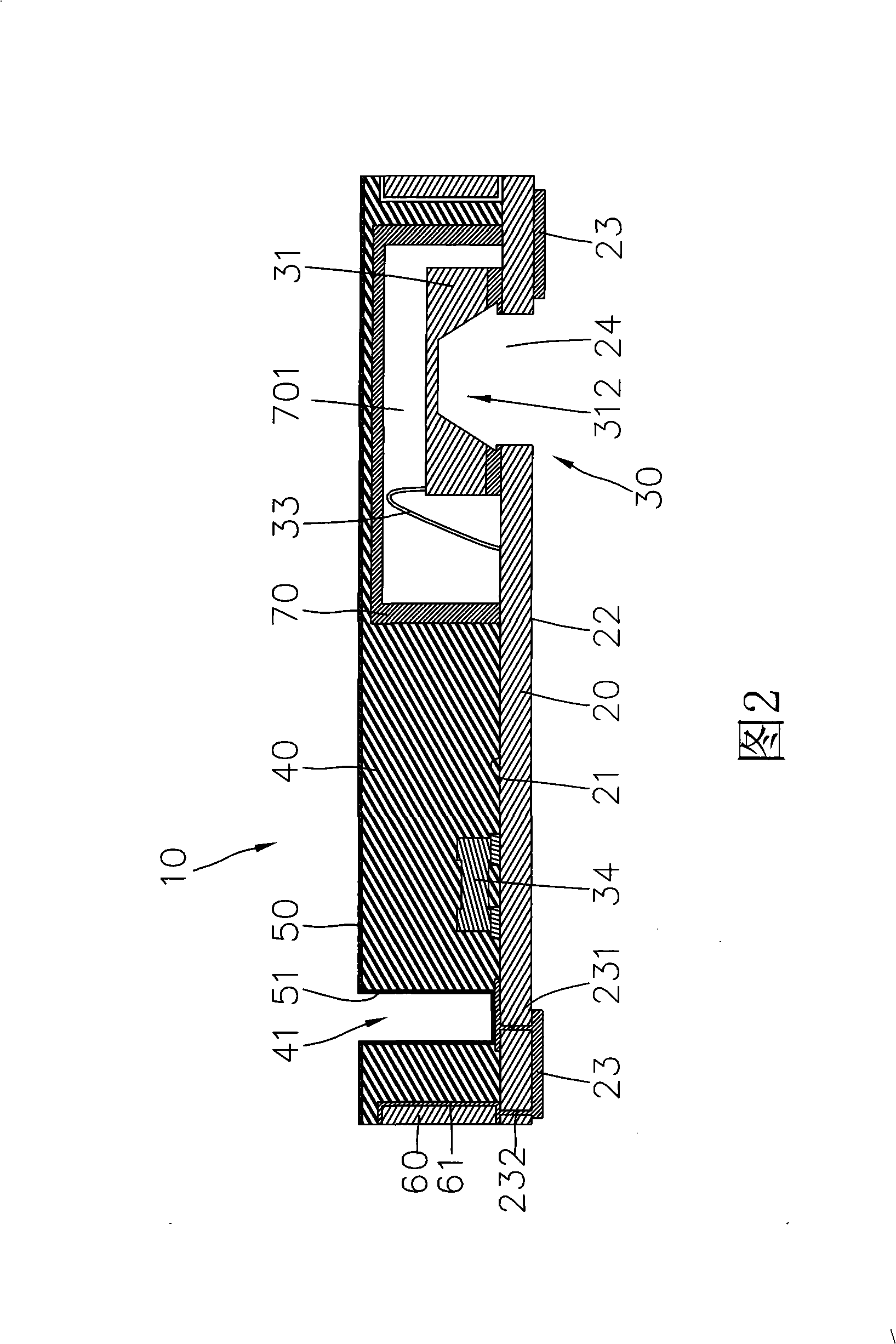
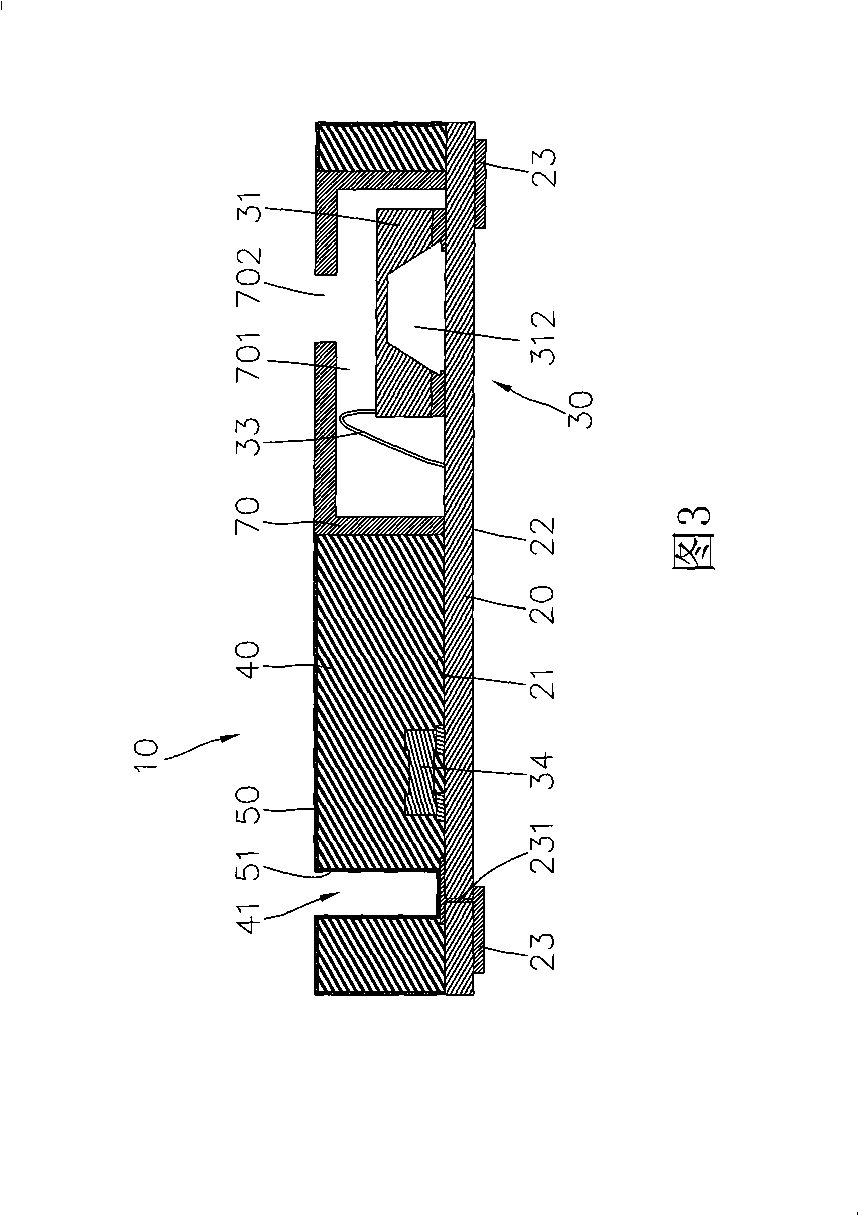
[0018] Referring to FIG. 1 , it is a schematic diagram of a first embodiment of the packaging structure of a silicon microphone according to the present invention. The packaging structure 10 of the silicon crystal microphone in this embodiment includes a substrate 20, an electronic component assembly 30 disposed on the substrate 20, a cover body 70 covering the electronic component assembly 30, a cover body 70 combined on the substrate 20 and covering The insulating filler 40 on the outer surface of the cover 70 , and a conductive layer 50 covering the outer surface of the insulating filler 40 .

[0019] The substrate 20 has an upper surface 21 and a lower surface 22. The upper surface 21 is used to hold the electronic component assembly 30, and the lower surface 22 is provided with soldering pads 23 at predetermined positions for electrical connection between the substrate 20 and the circuit board of the electronic product. And the pad 23 has a connecting portion 231 connecte...


PUM


Abstract

The invention discloses an encapsulation structure of a silicon crystal microphone, which comprises a substrate, an electronic component set, a cover body, an insulated filling body and a conducting layer. The substrate has an upper surface and a lower surface. The electronic component set comprises a silicon crystal microphone arranged on the upper surface of the substrate. The cover is arranged on the upper surface of the substrate and covers the silicon crystal microphone. The insulated filling body is combined on the upper surface of the substrate and the circumference side of the cover body, and provided with a hole communicating with the upper surface of the substrate. In addition, the conducting layer is formed out of the insulated filling body, and the hole of the insulated filling body is provided with a conducting part so as to electrically connect with the substrate.

Description

technical field [0001] The present invention mainly discloses a package structure of a microphone, especially a package structure of a silicon crystal microphone with good insulation and high signal-to-noise ratio. Background technique [0002] Please refer to FIG. 5 , which is a schematic view showing the package structure disclosed in US Patent No. U.S. 6,781,231. As shown in Figure 5, the package structure includes a substrate 1, on which a cup-shaped upper cover 2 is welded, and the upper cover 2 is composed of an outer cup 3 and an inner cup 4 , to form a shield for electromagnetic waves. A cavity 5 is formed between the upper cover 2 and the base plate 1 for several electronic components 6 to be accommodated on the base plate 1. In addition, the upper cover 2 is provided with several openings 7 for sound to enter the cavity 5, so that the Some electronic components 6 are able to receive the sound transmitted from outside the package structure. [0003] The above-men...

Claims


Application Information

Patent Timeline
Patent Type & Authority Applications(China)
IPC IPC(8): H04R31/00
CPCH01L2224/48091H01L2224/73265H01L2924/15151H01L2924/00014
Inventor 魏文杰何鸿钧龚诗钦张志伟
Owner MERRY ELECTRONICS CO LTD
Why Eureka
Try Eureka