Semiconductor integrated circuit and electronic apparatus having the same

A technology for integrated circuits and electronic equipment, applied in the field of electronic equipment, can solve the problems of complex manufacturing, complex BGA electrode structure IC manufacturing, etc., and achieve the effect of easy packaging process

Inactive Publication Date: 2005-03-30
ROHM CO LTD
View PDF1 Cites 15 Cited by
  • Summary
  • Abstract
  • Description
  • Claims
  • Application Information

AI Technical Summary

Problems solved by technology

Therefore, the manufacture of ICs with BGA electrode structure becomes complicated, which may cause new problems

Method used


Image

  • Semiconductor integrated circuit and electronic apparatus having the same
  • Semiconductor integrated circuit and electronic apparatus having the same
  • Semiconductor integrated circuit and electronic apparatus having the same

Examples


Embodiment Construction

[0030] Embodiments of the IC of the present invention and electronic equipment incorporating the IC will be described below with reference to the drawings. Figure 1-4 A first embodiment of the invention is shown.

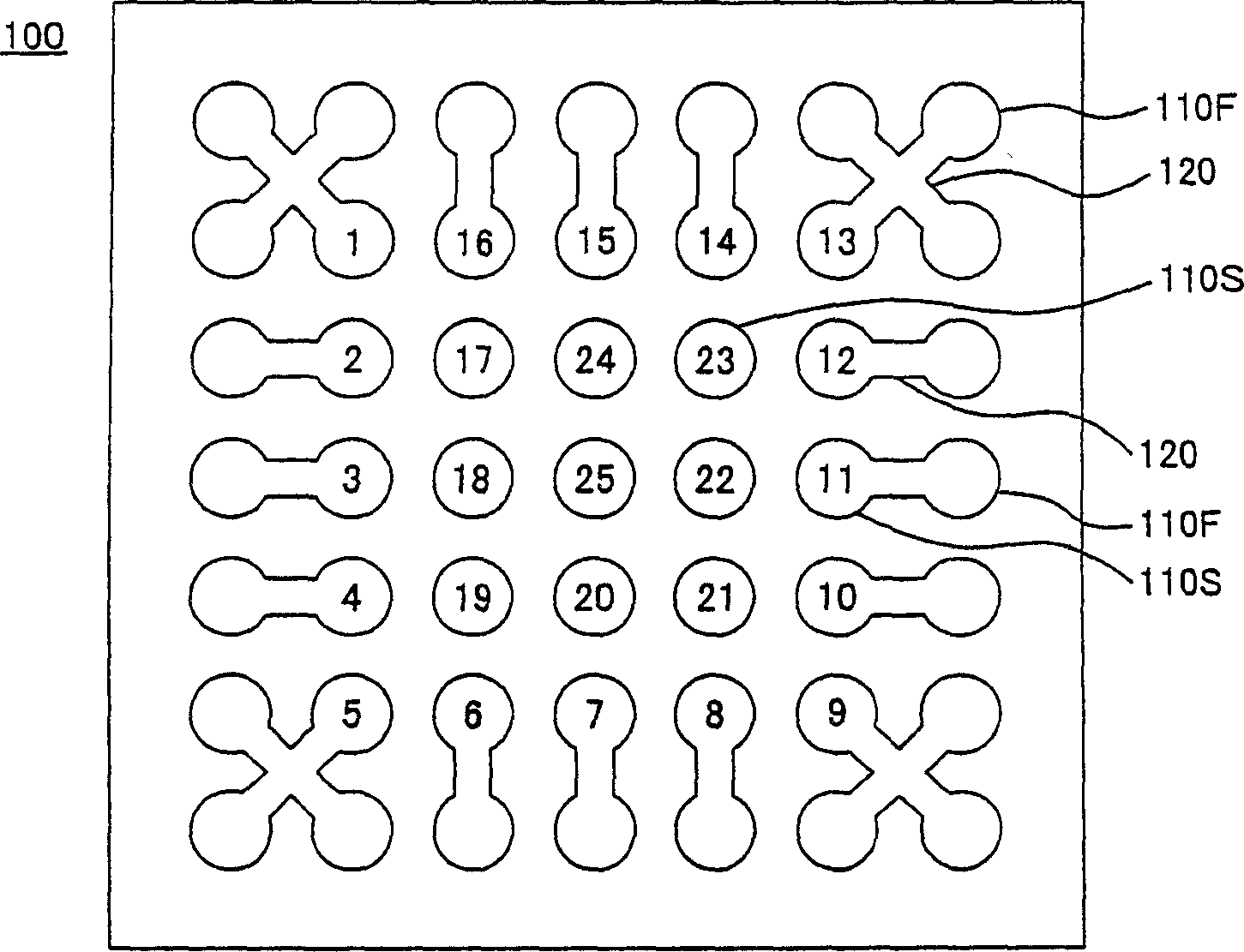
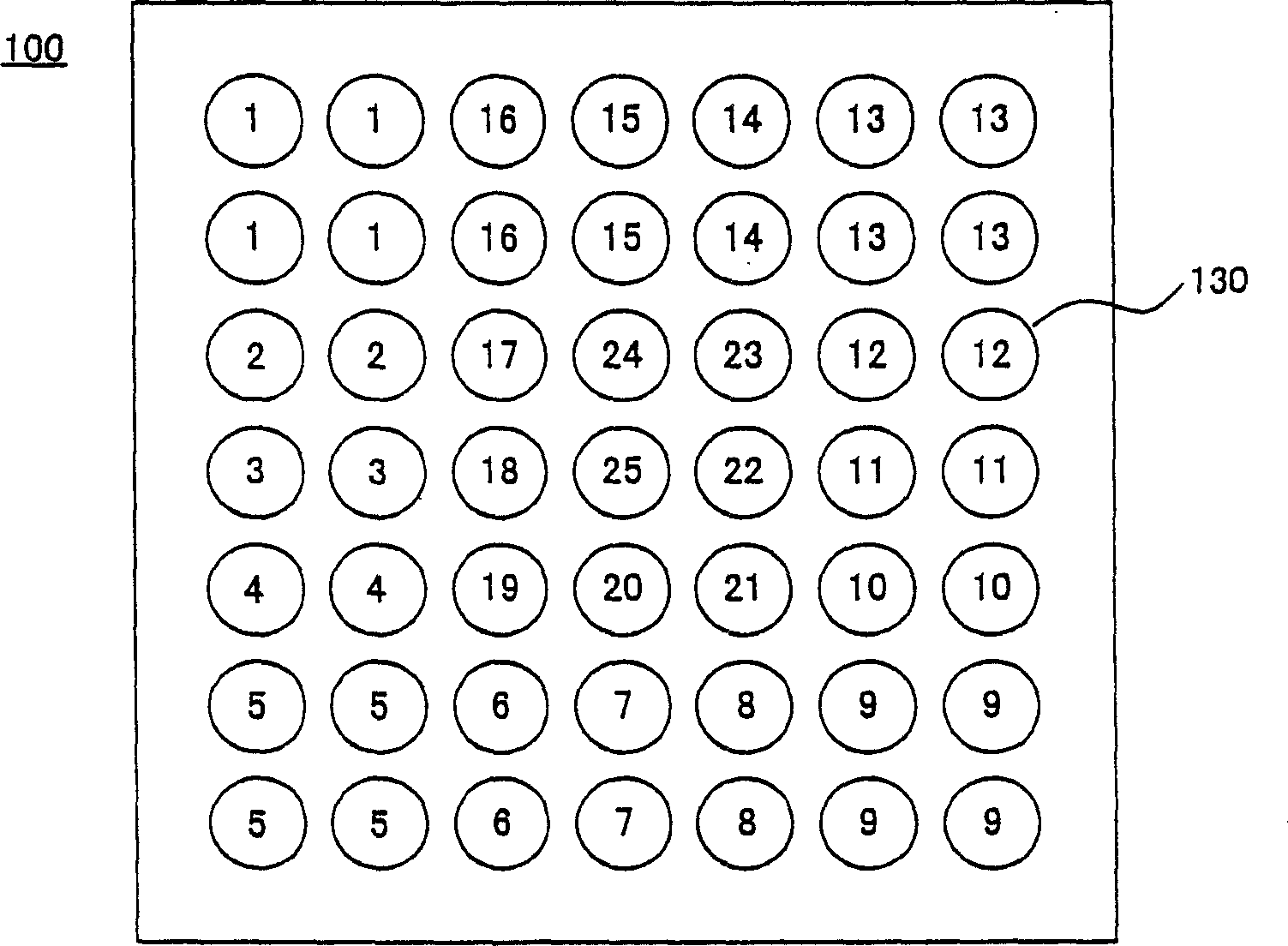
[0031] figure 1 A pattern of pads arranged in a grid array on one main surface side of the IC of the present invention is shown, figure 2 Figures of bumps provided on such pads are shown. image 3shows the installation figure 1 with figure 2 The electrode (pad) pattern on the mounting substrate of the IC. Figure 4 A schematic cross-sectional view showing a state where the IC of the present invention is mounted on a mounting substrate.

[0032] see figure 1 , in the IC 100, a plurality of pads 110 having substantially the same size are arranged in a grid on a predetermined area on one surface. The area is formed in a rectangular shape. As the rectangle, it may be a square as shown in the drawing, or may be a rectangle. The number of pads 110 is not limit...


PUM


Abstract

An IC has a multiplicity of electrodes or terminals arranged in a grid array configuration. The IC is provided with a multiplicity of pads in a similar grid array configuration. The pads other than the outermost pads of the array are used as signal pads. The outermost pads are used as reinforcing pads, which are connected to the signal pads adjacent the reinforcing pads. Bumps provided on the reinforcing pads and on the signal pads connected to the reinforcing pads are connected to associated bumps en bloc on an assembly board, thereby allowing the IC to be bonded to the assembly board with sufficient mechanical strength.

Description

technical field [0001] The present invention relates to a semiconductor integrated circuit device in which terminals are arranged in a grid array and electronic equipment incorporating the semiconductor integrated circuit device. Background technique [0002] A semiconductor integrated circuit device (hereinafter referred to as IC) accommodates and packages a semiconductor integrated circuit chip body. Among the terminal structures of such an IC is a ball grid array (BGA) electrode structure. The BGA electrode structure is such that electrode bumps (hereinafter referred to as bumps) formed of solder balls are provided in a grid array shape on one main surface of an IC. For an IC with a BGA electrode structure, multi-terminalization is easy, and the external dimensions can be configured to approximate the chip size. Therefore, an IC with BGA electrode configuration is called a chip scale package (CSP). In addition, the area of ​​a mounting substrate such as a printed wirin...

Claims


Application Information

Patent Timeline
Patent Type & Authority Applications(China)
IPC IPC(8): H01L23/12H01L21/60H01L23/485H01L23/498H01L23/50H05K1/11H05K3/34
CPCH01L24/14H01L2924/14H01L24/10H01L2924/01002H01L2224/16H05K3/3436H01L24/73H01L2224/81801H01L2924/01082H05K1/113H05K2201/10734H01L2224/13099H01L2924/014H01L23/49838H01L2924/19043H01L23/49816H01L2924/01006H01L2924/01033H05K1/111H05K2201/094H01L2924/19041H01L23/50H01L2924/01079H01L24/81H01L24/05H01L24/06H01L24/09H01L24/13H01L24/16H01L24/17H01L2224/02375H01L2224/05571H01L2224/05573H01L2224/06517H01L2224/09517H01L2224/13H01L2224/14131H01L2224/16227H01L2224/17107H01L2224/17517H01L2924/351Y02P70/50H01L2924/00H01L21/60
Inventor 长尾充大
Owner ROHM CO LTD
Why Eureka
Try Eureka