Chip encapsulation structure and technology

A chip packaging structure and chip packaging technology, applied to electrical components, electrical solid devices, circuits, etc., can solve problems such as package deformation, chip and substrate alignment inaccuracy, chip pad damage, etc., to reduce substrate warpage , Improving the pass rate and the effect of product reliability

Inactive Publication Date: 2010-01-27
IND TECH RES INST
View PDF4 Cites 0 Cited by
  • Summary
  • Abstract
  • Description
  • Claims
  • Application Information

AI Technical Summary

Problems solved by technology

Moreover, with the miniaturization of the chip packaging structure and the improvement of circuit integration, the above-mentioned thermal stress effect will become more obvious, which may cause serious warpage of the substrate and cause solder pads on the chip during the process. Problems such as damage, misalignment between chips and substrates, etc.
In more serious cases, it will cause the chip to be delaminated from the substrate and the package to be deformed (out of spec), which will affect the normal operation of the chip and the pass rate of the packaging process.

Method used


Image

  • Chip encapsulation structure and technology
  • Chip encapsulation structure and technology
  • Chip encapsulation structure and technology

Examples


Embodiment Construction

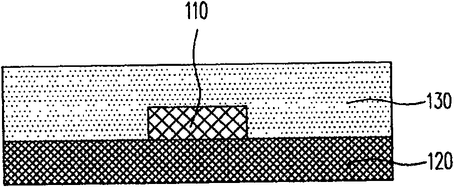
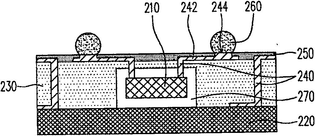
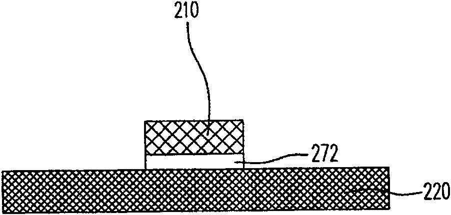
[0048] figure 2 A chip package structure is shown as a preferred embodiment of the present invention. Such as figure 2 As shown, in order to provide a stress buffering effect on the chip 210 , the present invention provides a buffer colloid 270 around the chip 210 , and the chip is disposed on the substrate 220 through the buffer colloid 270 . In addition, the encapsulant 230 covers the buffer 270 and the chip 210 , and a plurality of interconnections 240 are formed in the buffer 270 and the encapsulant 230 .

[0049] please refer again figure 2 Part of the interconnection 240 is connected to the surface circuit 242 on the surface of the encapsulant 230 , and the surface of the encapsulant 230 is provided with a protective layer 250 , which exposes a part of the surface circuit 242 as a plurality of contacts 244 . In addition, solder balls 260 are disposed on the contacts 244 , and the chip 210 can be electrically connected to an external circuit (not shown in the figure...


PUM


Abstract

This invention provides one chip sealing structure, which comprises chip and buffer glue, wherein, the chip has main surface, back surface and multiple sides in between, wherein, the buffer glue is set on main and back surfaces with buffer glue Yang mode less between 1Mpa and 1Gpa to reduce heat stress force and to improve chip sealing structure reliability. This invention also provides one chip sealing process to form buffer glue to get best process final product rate.

Description

technical field [0001] The invention relates to a semiconductor element and a manufacturing method thereof, and in particular to a chip packaging structure and a chip packaging process. Background technique [0002] In recent years, due to the rapid development of electronic technology and the rise of the semiconductor industry, electronic products that are more humane and better in function are constantly being introduced, and are designed towards the trend of light, thin, short and small. In the semiconductor industry, the purpose of chip packaging is to prevent the bare chip from being affected by moisture, heat and noise, and to provide electrical connection between the bare chip and external circuits, such as printed circuit boards (Printed Circuit Board, PCB) or other packaging substrates medium. [0003] Please refer to figure 1 , which represents a known chip packaging structure. The chip packaging structure 100 includes a chip 110, a substrate 120, and an encapsu...

Claims


Application Information

Patent Timeline
Patent Type & Authority Patents(China)
IPC IPC(8): H01L23/28H01L21/56
CPCH01L24/19H01L2224/04105H01L2224/12105H01L2224/19H01L2224/73267H01L2224/92244H01L2924/351H01L2924/00H01L2924/00012
Inventor 江家雯陈守龙
Owner IND TECH RES INST
Why Eureka
Try Eureka