

Micro- machining gas sensor and method for making same
A gas-sensing element and micro-machining technology, applied in the field of gas-sensing sensors, can solve the problem that the components cannot be miniaturized, and achieve the effect of reducing the area of the components, reducing the manufacturing cost, and simplifying the packaging process
- Summary
- Abstract
- Description
- Claims
- Application Information
AI Technical Summary
Problems solved by technology
Method used
Image

Examples
preparation example Construction
[0017] The preparation method of the above micro-processed gas sensor comprises the following steps:
[0018] First, the microelectrodes are fabricated on the substrate through micromachining technology. Micro-processing technology can use existing technologies, including: optical lithography, electron beam lithography, X-ray lithography, laser lithography, electrochemical corrosion, microparticle spraying, screen printing or film printing, etc. Existing technologies can be used to make microelectrode conductive materials, including: ion sputtering, electron beam evaporation, thermal evaporation, vacuum arc plasma coating, thermal spraying or electrostatic spraying, etc.
[0019] Then, cover the gas-sensitive material layer on the above-mentioned substrate and micro-electrodes to make a substrate component. The preparation method of the gas-sensitive material layer can adopt the existing technology, including sputtering, thermal evaporation, screen printing, aqueous solution ...
Embodiment 1
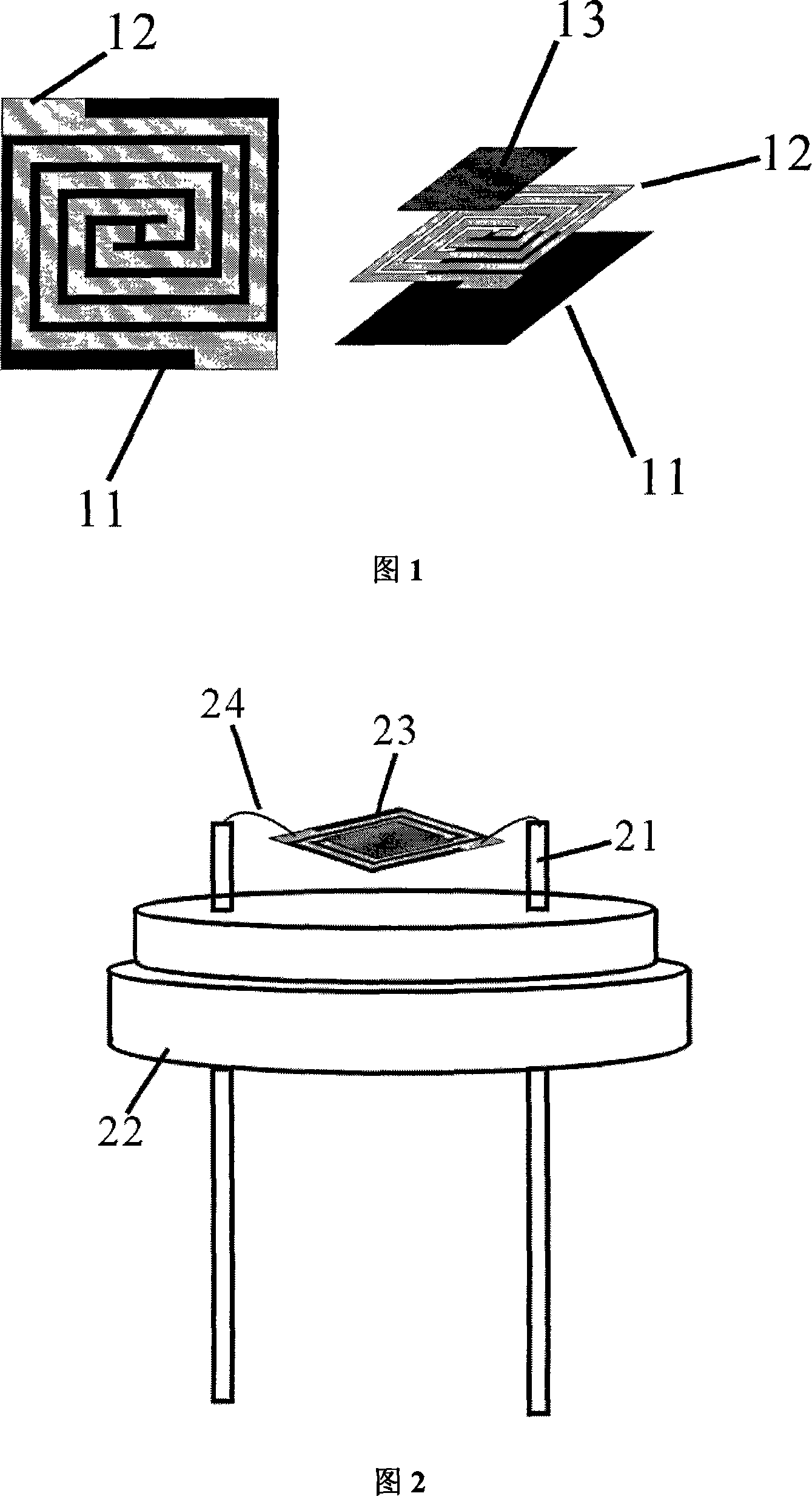
[0022] In this embodiment, a ceramic sheet with a thickness of 0.25mm is used as the substrate 11, and the unit area of the substrate is 1.5×1.5mm 2 . The microelectrode 12 is a single pair spaced back-shaped wire structure with a line width of 0.1 mm and a line spacing of 50 μm. The preparation method comprises the following steps:
[0023] a. The substrate 11 is pre-baked on a hot plate for 30 minutes, and the pre-baking temperature is 120° C.
[0024] b. A layer of Ruihong (RZJ-390PG) positive photoresist was evenly spin-coated on the surface of the substrate 11 with a Karl Suss R8 coating machine, and the coating speed was 3000 rpm for 60 seconds.
[0025] c. After gluing, place the substrate 11 on a hot plate for baking. The temperature of the hot plate is 120° C., and the baking time is 120 seconds.
[0026] d. After the baking is completed, use a Karl Suss MA45 photolithography machine to expose the sample to ultraviolet light for 15 seconds. During the exposure pr...
Embodiment 2
[0036] The steps of this embodiment are basically the same as those of Embodiment 1, except for the preparation of step j gas-sensitive material layer 13: In this embodiment, a layer of nanowires whose main component is tungsten oxide is grown on the substrate electrode by thermal evaporation to form film structure.
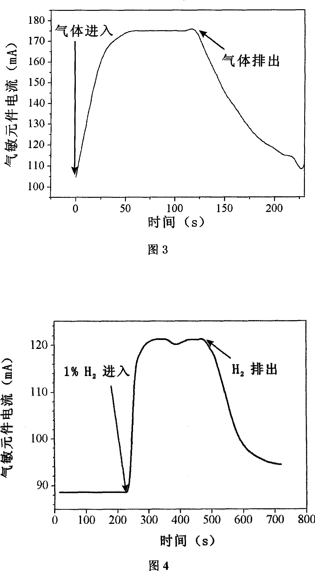
[0037] The gas sensing characteristic of this embodiment is shown in Fig. 4 . The gas sensor grown with tungsten oxide nanostructure material is 1% H under the condition of 2V DC power supply 2 The response current versus time curve. Among them, I represents the current flowing through the metal electrode, and t represents the time. When the device is in the air, its current value is about 89mA. When hydrogen gas appears, the current value of the device starts to increase, and reaches a stable value of about 120mA within 1 minute. When the hydrogen gas is discharged, the device current value begins to decrease, and finally falls back. to the original current v...
PUM
| Property | Measurement | Unit |
|---|---|---|
| Area | aaaaa | aaaaa |
| Thickness | aaaaa | aaaaa |
| Line width | aaaaa | aaaaa |
Abstract
Description
Claims
Application Information