Deep ultraviolet APD detection diode based on Ir2O3/Ga2O3 and manufacturing method thereof

A technology for detection diodes and manufacturing methods, which is applied in the field of deep ultraviolet APD detection diodes, can solve problems such as lack of withstand voltage and breakdown resistance, and achieve improved bulk avalanche breakdown voltage, high breakdown electric field, and high withstand voltage Effect

Active Publication Date: 2017-02-15
XIDIAN UNIV
View PDF2 Cites 15 Cited by
  • Summary
  • Abstract
  • Description
  • Claims
  • Application Information

AI Technical Summary

Problems solved by technology

[0004] However, the current APD detectors are not suitable for applications in extreme environments such as high frequency, high radiation, high temperature and high pressure because they do not have extremely high pressure resistance and breakdown resistance.

Method used


Image

  • Deep ultraviolet APD detection diode based on Ir2O3/Ga2O3 and manufacturing method thereof
  • Deep ultraviolet APD detection diode based on Ir2O3/Ga2O3 and manufacturing method thereof
  • Deep ultraviolet APD detection diode based on Ir2O3/Ga2O3 and manufacturing method thereof

Examples


Embodiment 1

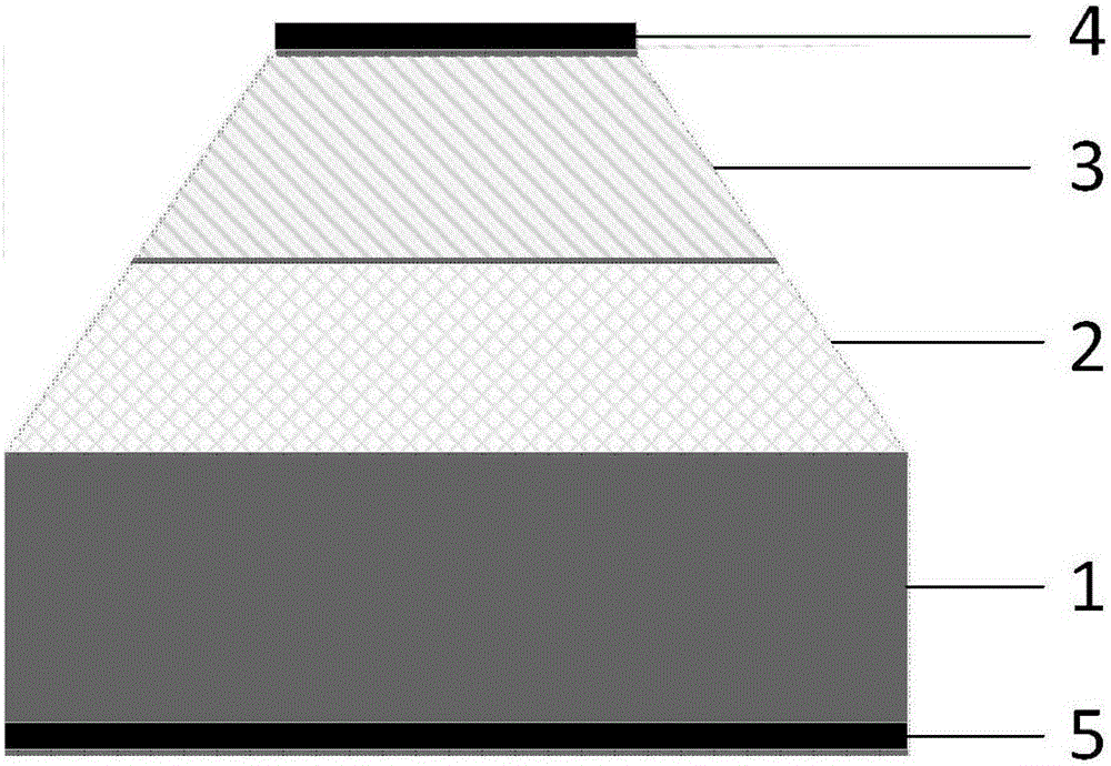
[0048] Wide bandgap semiconductor material Ga 2 o 3 , because the light transmittance of the material in the solar blind area can reach 80% or even more than 90%, it is very suitable for the photoelectric detection of the deep ultraviolet light solar blind area. Its photoelectric sensitivity is high, and it has both the transparency of sapphire and the conductivity of SiC. It is an ideal semiconductor material for the study of devices, especially deep ultraviolet photodetectors.

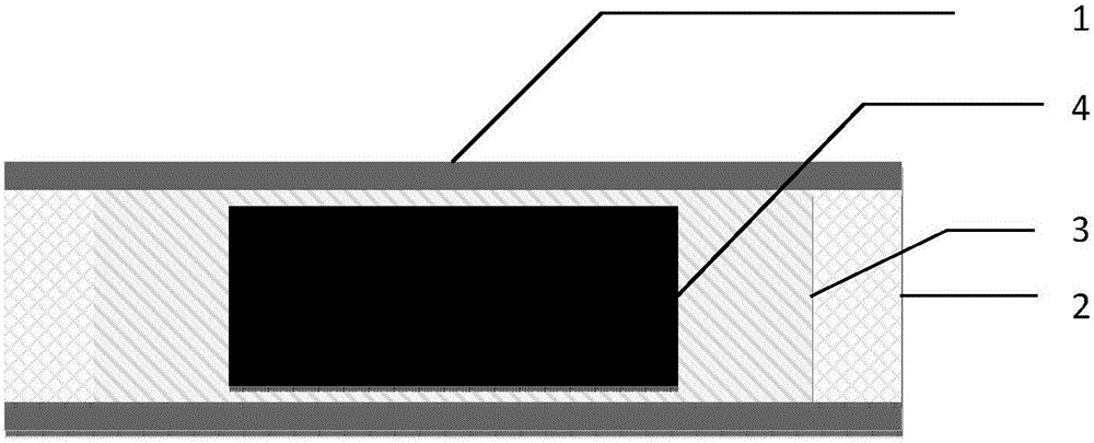
[0049] See figure 1 and figure 2 , figure 1 A kind of based on Ir provided for the embodiment of the present invention 2 o 3 / Ga 2 o 3 The cross-sectional schematic diagram of the deep ultraviolet APD detection diode; figure 2 A kind of based on Ir provided for the embodiment of the present invention 2 o 3 / Ga 2 o 3 The schematic top view of the deep ultraviolet APD detection diode. The APD detection diode consists of β-Ga 2 o 3 Composed of a substrate 1, an N-type homoepitaxial laye...

Embodiment 2

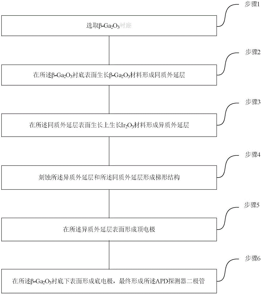
[0080] See Figure 4a-Figure 4g and Figure 5 , Image 6 with Figure 7 . Figure 4a-Figure 4g A kind of based on Ir provided for the embodiment of the present invention 2 o 3 / Ga 2 o 3 Schematic diagram of the fabrication method of the deep ultraviolet APD detection diode; Figure 5 A schematic diagram of a first photolithography mask provided by an embodiment of the present invention; Image 6 A schematic diagram of a second photolithography mask provided by an embodiment of the present invention; and Figure 7 A schematic diagram of a third photolithography mask provided by an embodiment of the present invention. On the basis of the above-mentioned embodiments, this embodiment is based on the Ir 2 o 3 / Ga 2 o 3 The fabrication method of the deep ultraviolet APD detection diode is described in detail as follows:

[0081] Step 1: See Figure 4a , to prepare the substrate for β-Ga 2 o 3 , the thickness is 200 μm-600 μm, and the substrate is pretreated and clea...


PUM

PropertyMeasurementUnit
transmittivityaaaaaaaaaa

Abstract

The invention relates to a deep ultraviolet APD detection diode based on Ir2O3/Ga2O3 and a manufacturing method thereof. The method comprises the following steps of selecting a beta-Ga2O3 substrate; growing a beta-Ga2O3 material on a beta-Ga2O3 substrate surface to form a homogeneous epitaxial layer; growing an Ir2O3 material on a homogeneous epitaxial layer surface so as to form a heterogeneous epitaxial layer; etching the heterogeneous epitaxial layer and the homogeneous epitaxial layer to form a trapezoidal structure; forming a top electrode on a heterogeneous epitaxial layer surface; and forming a bottom electrode on a lower surface of the beta-Ga2O3 substrate and finally forming an APD detector diode. In the invention, the beta-Ga2O3 material is used, a super high light penetration rate and transparency of the material in a deep ultraviolet area and a visible light area are performed, super high voltage withstanding performance of an APD detector and a high breakdown electric field are ensured; the diode is suitable for extreme environments of a high frequency, high radiation, high temperature and high voltage and the like; under the extreme environments, device reliability can be greatly increased and detection performance is better than that of an existing APD detector.

Description

technical field [0001] The invention belongs to the technical field of integrated circuits, in particular to an Ir-based 2 o 3 / Ga 2 o 3 A deep ultraviolet APD detection diode and a fabrication method thereof. Background technique [0002] With the continuous deepening of research and exploration work in the fields of astronomy, high-energy physics, and space technology in recent years, and the rapid expansion of application prospects in space exploration, artificial satellites, etc., the requirements for light detectors, especially ultraviolet light, are increasing. The higher it is, the more attention the military has on technologies such as photoelectric countermeasures, mid-ultraviolet countermeasures and anti-resistance technologies. Usually, electromagnetic waves with a wavelength of 10-400nm become ultraviolet rays, which are different from visible light radiation and infrared radiation. Among them, the spectral region in the ultraviolet rays from solar radiation ...

Claims


Application Information

Patent Timeline
Patent Type & Authority Applications(China)
IPC IPC(8): H01L31/18H01L31/107H01L31/032
CPCH01L31/032H01L31/1075H01L31/18
Inventor 元磊张弘鹏贾仁需张玉明
Owner XIDIAN UNIV
Why Eureka
Try Eureka