Circuit board processing method

A processing method and circuit board technology, applied in printed circuit, printed circuit manufacturing, electrical components, etc., can solve the problems of increasing process difficulty, reducing yield rate, increasing cost, etc., to expand the area of ​​wiring area, reduce wiring density, improve The effect of product yield

Inactive Publication Date: 2012-02-22
SHENZHEN WUZHU TECH +1
View PDF2 Cites 3 Cited by
  • Summary
  • Abstract
  • Description
  • Claims
  • Application Information

AI Technical Summary

Problems solved by technology

[0009] However, using the screw 91 to pass through the positioning hole 83 and the through hole 93 at the same time to locate the positioning jig 90 will increase the difficulty of the process because of the need for drilling, alignment, etc., and due to the limitation of the processing technology, how to accurately align bit becomes a new challenge
In addition, if it is necessary to arrange dense conductive lines on the surface of the circuit board 80, or even cut the circuit board 80, the existence of the positioning hole 83 will inevitably make the wiring accuracy and cutting process more demanding, and more complicated, and it is easy to cut the circuit board 80 in the positioning hole. Cracks or burrs appear at the place, increasing cost and reducing yield

Method used


Image

  • Circuit board processing method
  • Circuit board processing method
  • Circuit board processing method

Examples


Embodiment Construction

[0029] The specific embodiments of the present invention will be described in detail below with reference to the accompanying drawings.

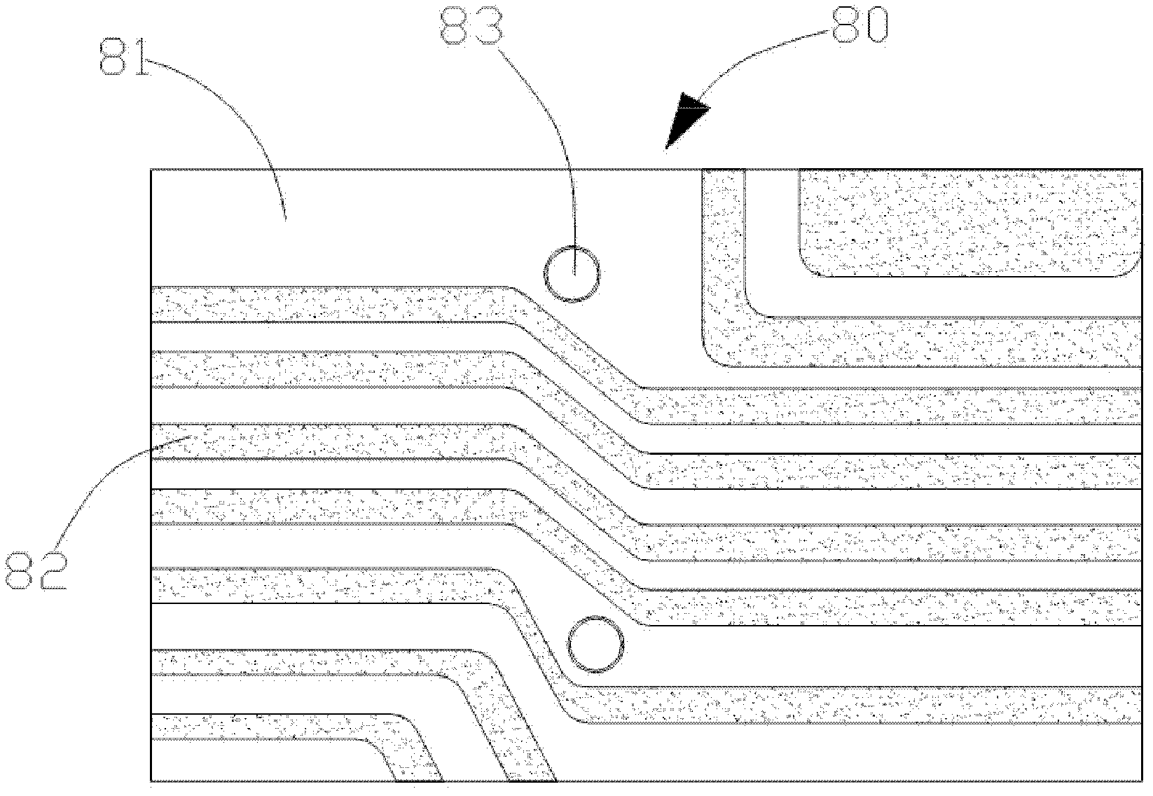
[0030] Circuit boards can be divided into single-sided, double-sided and multi-layer boards according to their wiring levels. A single-sided circuit board is a printed board that is provided with conductive patterns on only one surface. Generally, it is made of phenolic paper-based copper-clad foil layer, and epoxy paper-based or epoxy glass cloth copper-clad laminate is often used.

[0031] The printed pattern of the single-sided circuit board is relatively simple. Generally, the method of screen printing is used to transfer the pattern, and then the printed board is etched, and some are produced by the photochemical method.

[0032] A double-sided circuit board is a printed board with conductive patterns arranged on the opposite sides. Obviously, the area of ​​a double-sided circuit board is twice as large as that of a single-sided board...


PUM


Abstract

The invention relates to a circuit board processing method, which comprises the following steps of: providing a cutting platform with a gas path, providing medium layers, overlapping the medium layers on the surface of the cutting platform, providing a circuit board, pressing the circuit board on the medium layer, providing a vacuumizing device, vacuumizing gas among the cutting platform and the medium layers so that a vacuum environment is formed from the cutting platform to the circuit board, and realizing adsorption and fixation among the circuit board and various medium layers. According to the method disclosed by the invention, the circuit board is fixed in a vacuum adsorption manner; a locating hole is not used; the problems of high cost, poor cutting effect and complex circuit design resulted from the arrangement of the locating hole can be effectively solved; and the locating effect is increased.

Description

technical field [0001] The invention relates to a functional device for realizing electrical connection between components and signal processing, in particular to a processing method of a circuit board. Background technique [0002] Printed Circuit Board (PCB) is the basis of almost any electronic product and appears in various electronic devices. Generally speaking, if there are electronic components in a device, they are also installed in different sizes. circuit board surface. [0003] In addition to fixing various components, the main function of the circuit board is to provide the connection circuit between the components. As electronic devices become more and more complex, more and more components are required, and the lines and components on the surface of the PCB are becoming more and more dense. [0004] The circuit board itself is made of insulating and heat-insulating material, and conductive lines and functional components are arranged on its surface, wherein t...

Claims


Application Information

Patent Timeline
Patent Type & Authority Applications(China)
IPC IPC(8): H05K3/00
Inventor 徐学军
Owner SHENZHEN WUZHU TECH
Why Eureka
Try Eureka