Printed circuit board (PCB) processing method

A processing method and circuit board technology, applied in the direction of multi-layer circuit manufacturing, etc., can solve the problems of increasing production costs, waste of resources, pollution of holes 820, etc., and achieve the effects of saving production costs, meeting shape requirements, and ensuring functional integrity

Active Publication Date: 2012-02-29
SHENZHEN WUZHU TECH +1
View PDF3 Cites 11 Cited by
  • Summary
  • Abstract
  • Description
  • Claims
  • Application Information

AI Technical Summary

Problems solved by technology

[0010] However, during the heating process, the hot pressing device 85 needs to apply a pressing force downward, so that the pressing between the laminates 81, 82 is more compact, and the silicone sheet 84 and the adhesive sheet 86, so that the molten fluid of the bonding sheet 86 or the silicone sheet 84 overflows in the hole 820, and is extruded into the gap between the filled silica gel 83 and the hole 820. , causing pollution to the hole 820, affecting the performance of the circuit board
At the same time, the silica gel sheet 84 is not easy to recycle and reuse, resulting in waste of resources and increased production costs

Method used


Image

  • Printed circuit board (PCB) processing method
  • Printed circuit board (PCB) processing method
  • Printed circuit board (PCB) processing method

Examples


Embodiment Construction

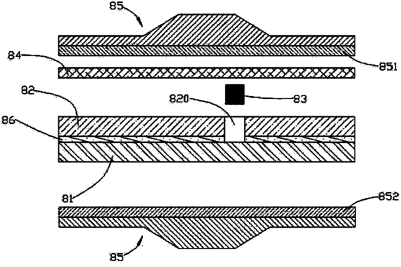
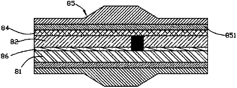
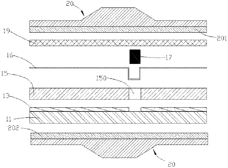
[0027] Specific embodiments of the present invention will be described in detail below in conjunction with the accompanying drawings.

[0028] Circuit boards can be divided into single-panel, double-panel and multi-layer boards according to their wiring levels. A single-sided board is a circuit board with conductive patterns on only one side. It is generally made of phenolic paper-based copper clad laminates, and epoxy paper-based or epoxy glass cloth copper clad laminates are often used.

[0029] The printed graphics of single-sided panels are relatively simple. Generally, the screen printing method is used to transfer the graphics, and then the circuit board is etched out, and some are produced by photochemical methods.

[0030] Double-sided circuit boards are circuit boards with conductive patterns on both sides. Obviously, the area of ​​the double-sided panel is twice as large as that of the single-sided panel, and it is suitable for more complex circuits than the single...


PUM


Abstract

The invention relates to a printed circuit board (PCB) processing method. The method comprises the following steps: providing a first laminate; providing a second laminate which comprises a plurality of holes and placing the second laminate on a first laminate surface, wherein the hole can correspondingly form a concave structure after the second laminate is placed on the first laminate surface; isolation films are placed on an upper surface of the second laminate and an inner wall of the concave structure; filling a filler in the holes; a high temperature silicon sheet is placed on the uppersurface of the second laminate; providing hot-pressing equipment and carrying out hot-pressing processing to the hot-pressing equipment, the first laminate, the isolation films and the second laminate; removing the high temperature silicon sheet, the filler and the isolation films so as to form a multilayer board with the concave structure. By using the PCB processing method of the invention, thefiller and high temperature silica gel are isolated with the holes of the second laminate through the isolation films so that a bonding sheet or the high temperature silica gel can be prevented from infiltrating into the holes during a hot-pressing process and hole function completeness can be ensured. The high temperature silica gel can be recycled and production costs can be saved.

Description

technical field [0001] The invention relates to a functional device for realizing electrical connection and signal processing between electronic components on the surface of a circuit board, in particular to a processing method for a circuit board. Background technique [0002] Printed Circuit Board (PCB) is the basis of almost any electronic product and appears in almost every electronic device. Generally speaking, if there are electronic components in a certain device, they are also installed on PCBs of various sizes. [0003] In addition to fixing various components, the main function of PCB is to provide connection circuits between various components. As electronic equipment becomes more and more complex, more and more components are required, and the arrangement of lines and components on the surface of PCB is becoming more and more dense. [0004] The plate itself of the printed circuit board is made of insulating and heat-insulating material that cannot be bent. The...

Claims


Application Information

Patent Timeline
Patent Type & Authority Applications(China)
IPC IPC(8): H05K3/46
Inventor 古建定徐学军
Owner SHENZHEN WUZHU TECH
Why Eureka
Try Eureka