
Method for processing substrates with process gas

A process gas and substrate technology, applied in post-processing, chemical instruments and methods, crystal growth, etc., can solve the problems of reduced productivity, uneven doping, and reduced number of wafers, achieving high productivity, good processing uniformity, The effect of making up for unevenness

Active Publication Date: 2013-12-11
FOUNDER MICROELECTRONICS INT
View PDF4 Cites 0 Cited by
  • Summary
  • Abstract
  • Description
  • Claims
  • Application Information

AI Technical Summary

Problems solved by technology

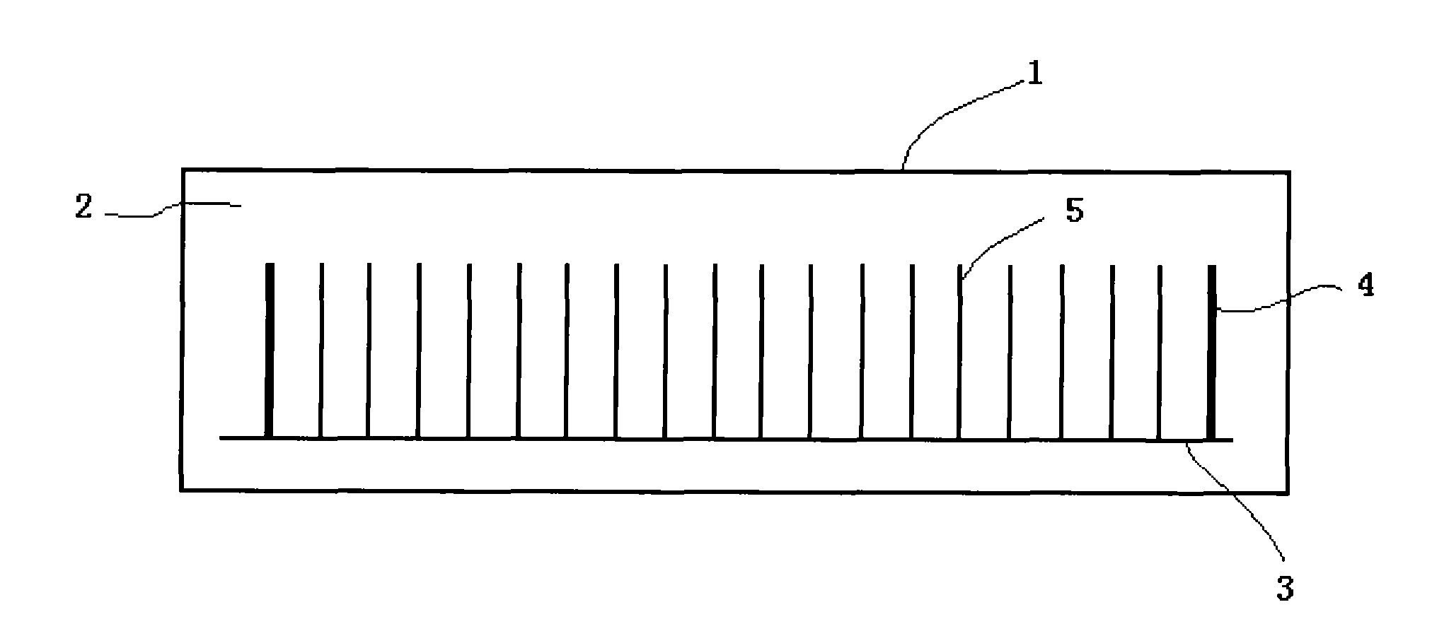
[0004] The inventor finds that there are at least the following problems in the prior art: if the interval between the wafers is small, the gas flow between the wafers will be greatly restricted, so that the amount of gas reaching the middle of the wafer in the reaction process is less than The amount of gas reaching the periphery of the wafer, so that the doping concentration in the middle of the wafer is lower than that in the periphery, resulting in uneven doping; and if the interval between the wafers is enlarged or the wafers are arranged in other ways , it will reduce the number of wafers that can be processed per furnace and reduce production capacity

Method used


Image

  • Method for processing substrates with process gas
  • Method for processing substrates with process gas
  • Method for processing substrates with process gas

Examples


Embodiment 1

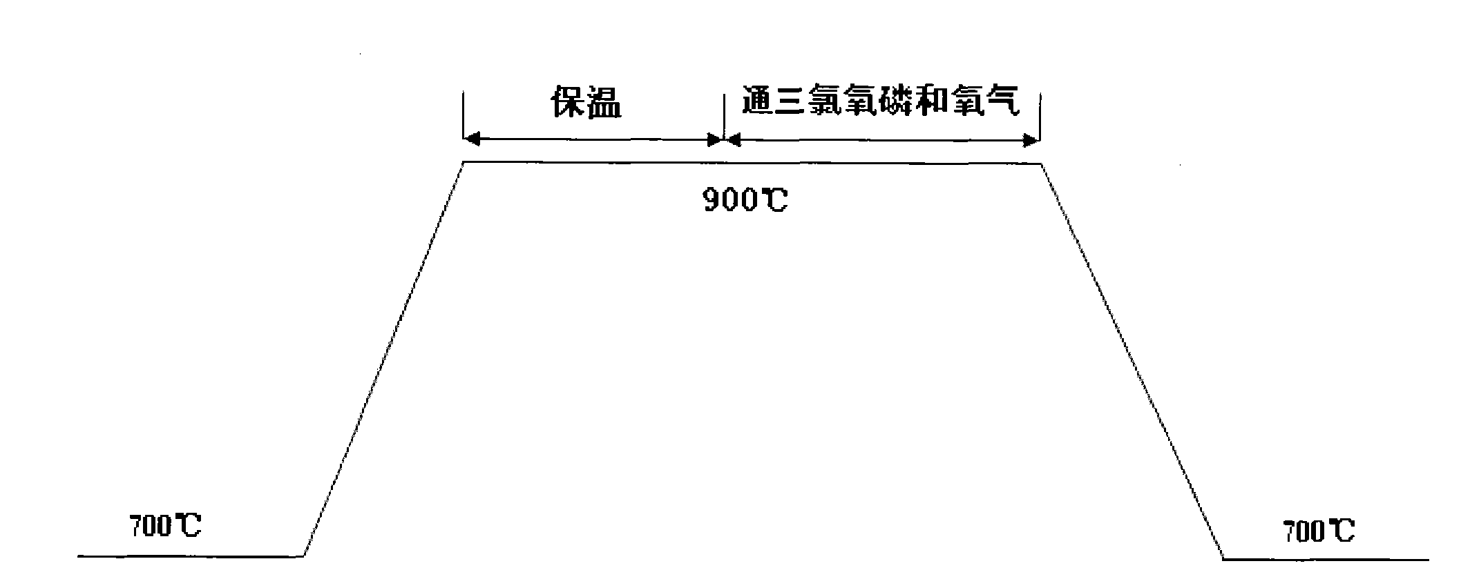
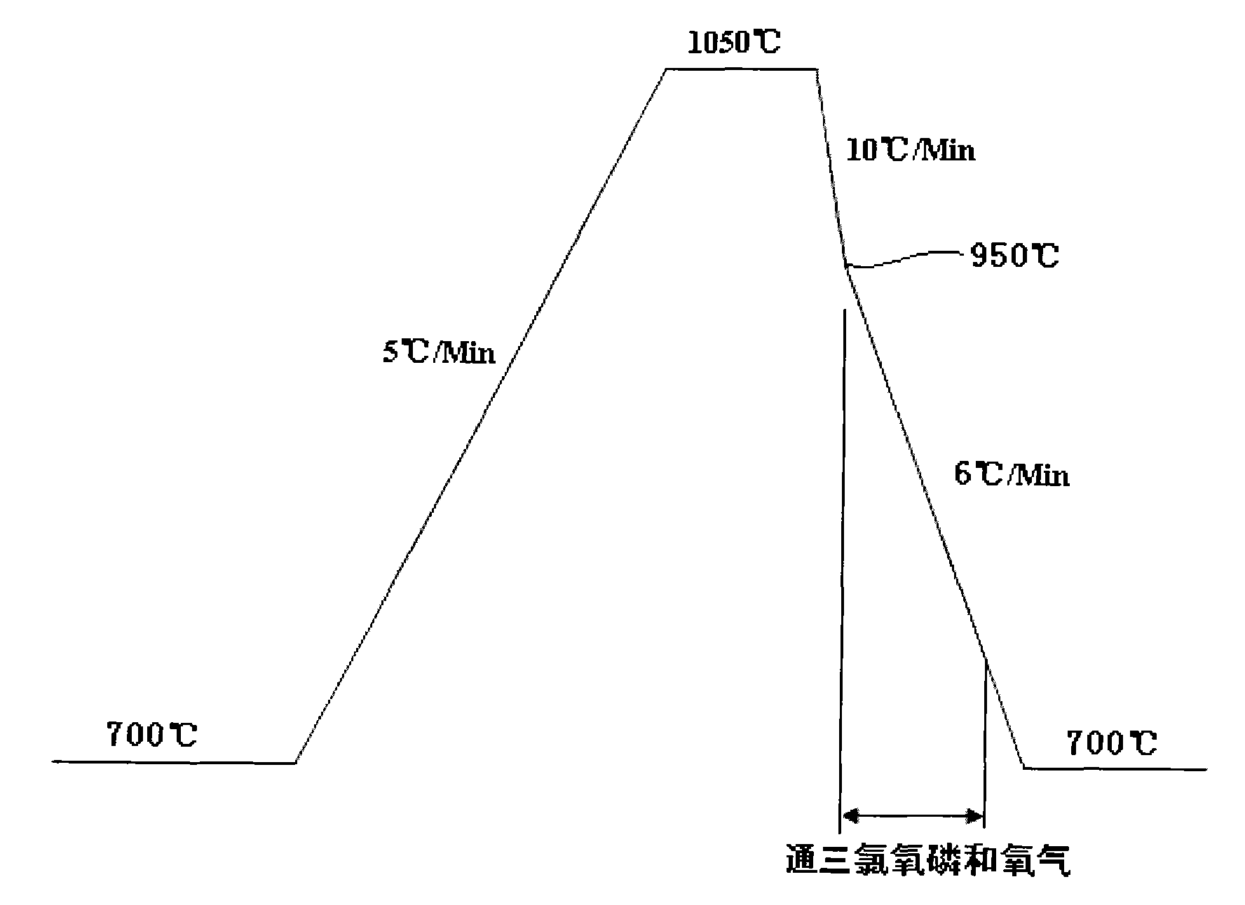
[0024] An embodiment of the present invention provides a method for doping a wafer with phosphorus oxychloride, which includes:

[0025] Step 1. At the standby temperature of 700°C, slowly move the quartz boat containing multiple wafers with a diameter of 6 inches into the chamber of the furnace tube. The wafers are arranged in a row opposite to each other on the upper surface of the quartz boat. The distance between the adjacent wafers is 4.76 millimeters, and a stopper is respectively set at the two ends of a row of wafers, and the distance between the stopper and the adjacent wafer is also 4.76 millimeters (the stoppers are set in this way to ensure that the wafers at the end of the row The outer surface of the wafer gets a uniform treatment).

[0026] Step 2. Heat the chamber of the furnace tube to 1050° C. at a heating rate of 5° C. / min.

[0027] Step 3, keeping the temperature at 1050° C. for 20 minutes to make the temperature of each part of each wafer uniform.

[002...

Embodiment 2

[0032] An embodiment of the present invention provides a method for growing polysilicon on a semiconductor substrate with silane gas, comprising:

[0033] Step 1. Slowly move the quartz boat containing multiple semiconductor substrates into the chamber of the furnace tube at a standby temperature of 600°C. The arrangement of the substrates is the same as that of the wafers in Embodiment 1.

[0034] Step 2. Heat the chamber of the furnace tube to 900° C. at a heating rate of 6° C. / min.

[0035] Step 3, keeping the temperature at 900° C. for 20 minutes, so that the temperature of each part of each semiconductor substrate is uniform.

[0036] Step 4, cooling the chamber to 700° C. at a cooling rate of 8° C. / min, so that the temperature in the middle of the semiconductor substrate is higher than that in the peripheral portion.

[0037] Step 5. When the temperature of the chamber is lowered to 700°C, feed silane into the chamber and start to cool the chamber at a cooling rate of 4...


PUM


Abstract

The invention provides a method for processing substrates with a process gas and belongs to the technical field of surface treatment. According to the method, the problem of a traditional method for processing the substrates with the process gas that excellent uniformity and high yield cannot be acquired at the same time can be solved. The method for processing the substrates with the process gas comprises the following steps: heating a chamber of a processing device which is provided with at least two to-be-processed substrates to be at a first temperature, and arranging the surfaces of the substrates into at least one row in the form of being face to face at intervals; cooling the chamber to be at a second temperature at a first cooling speed, wherein the first cooling speed is high enough to cause the temperature of the middle parts of the substrates to be higher than the temperature of the peripheral parts thereof; and under a condition that the temperature of the middle parts of the substrates is higher than the temperature of the peripheral parts thereof, introducing the process gas into the chamber for processing the substrates. The method provided by the invention can be applied to the field of semiconductor technology.

Description

technical field [0001] The invention relates to a method for treating a substrate with a process gas, in particular to a method for treating a substrate with a process gas used in the field of semiconductor technology. Background technique [0002] Treating a substrate with a process gas is a common process in the field of semiconductor processing. For example, with phosphorus oxychloride (PCLO 3 ) gas and oxygen to dope the wafer, in which phosphorus oxychloride reacts with oxygen to generate phosphorus pentoxide, and then phosphorus pentoxide reacts with silicon in the wafer to generate phosphorus, which diffuses into the wafer after annealing to form a conductive layer (N layer), to complete the doping. [0003] Such as figure 1 As shown, the existing phosphorus oxychloride doping is usually carried out in the furnace tube 1, and a plurality of wafers 5 are arranged on the quartz boat 3, and are arranged in a row along the chamber 2 of the furnace tube 1, and adjacent ...

Claims


Application Information

Patent Timeline
Patent Type & Authority Patents(China)
IPC IPC(8): C30B31/06
Inventor 徐威刘根冯超林徐家骏王冬梅
Owner FOUNDER MICROELECTRONICS INT
Learn More