
Method for preparing failure analysis sample

A technology for failure analysis of samples and samples, applied in the preparation of test samples, etc., can solve the problems of inability to provide analysis data, easy deformation of the structure to be analyzed, etc., to reduce interactions, eliminate surface charge effects, and effectively analyze data. Effect

Active Publication Date: 2014-03-12
SEMICON MFG INT (SHANGHAI) CORP +1
View PDF5 Cites 0 Cited by
  • Summary
  • Abstract
  • Description
  • Claims
  • Application Information

AI Technical Summary

Problems solved by technology

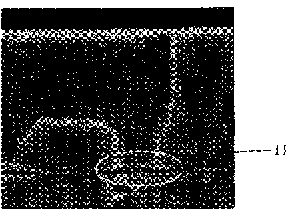
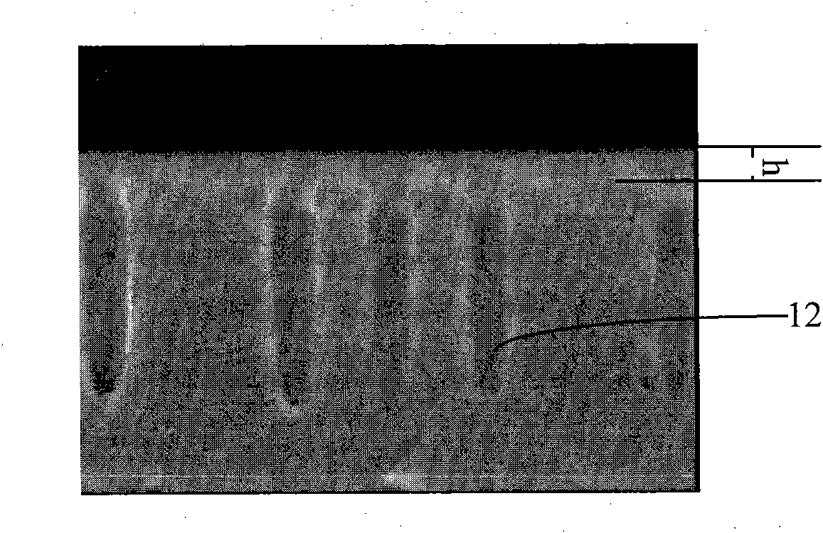
[0006] The problem to be solved by the present invention is that when using the analysis sample prepared by the existing method for failure analysis, the structure to be analyzed is easily deformed during the analysis process, and effective analysis data cannot be provided.

Method used


Image

  • Method for preparing failure analysis sample
  • Method for preparing failure analysis sample
  • Method for preparing failure analysis sample

Examples


Embodiment Construction

[0029] In the method for preparing a failure analysis sample according to a specific embodiment of the present invention, a protective layer is formed on the electron bombardment surface of the analysis structure, that is, a heavy metal with a first predetermined thickness is formed on the first surface, and a heavy metal with a second predetermined thickness is formed on the second surface. A heavy metal, selected from gold, platinum or chromium, protects the electron bombardment side of the analytical structure.

[0030] In order to enable those skilled in the art to better understand the present invention, the method for preparing a failure analysis sample according to a specific embodiment of the present invention will be described in detail below with reference to the accompanying drawings.

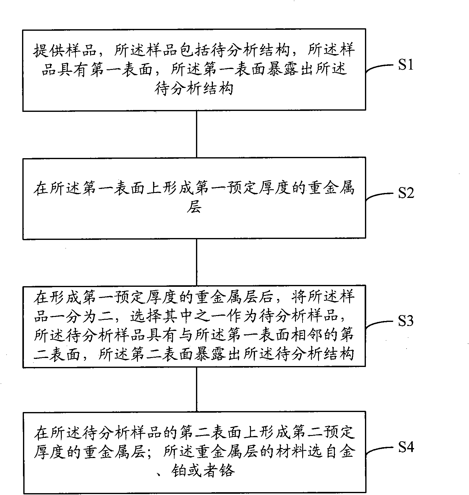
[0031] figure 2 It is the flowchart of the method for preparing the failure analysis sample of the specific embodiment of the present invention, refer to figure 2 , the method for...


PUM

PropertyMeasurementUnit
thicknessaaaaaaaaaa
thicknessaaaaaaaaaa
thicknessaaaaaaaaaa

Abstract

The invention discloses a method for preparing a failure analysis sample, which comprises a providing a sample, wherein the sample comprises a structure to be analyzed, and is provided with a first surface, the first surface is exposed out of the structure to be analyzed; forming a heavy metal layer with a first preset thickness on the first surface; after the heavy metal layer with the first preset thickness is formed, dividing the sample into two parts, selecting one part to be used as a sample to be analyzed, wherein the sample to be analyzed is provided with a second surface adjacent to the first surface, the second surface is exposed out of the structure to be analyzed; and forming a heavy metal layer with a second preset thickness on the second surface of the sample to be analyzed. The heavy metal layers are made of gold, platinum or chrome. When the sample prepared by using the method is subjected to the failure analysis, factors causing the deformation of a low-dielectric constant material and an ultra-low-dielectric constant material can be basically eliminated, original shapes of the sample can be kept and effective analysis data can be provided.

Description

technical field [0001] The invention relates to sample failure analysis in the technical field of semiconductors, in particular to a method for preparing samples for failure analysis. Background technique [0002] In the field of semiconductor technology, when using semiconductor technology to manufacture semiconductor devices, due to process defects in the semiconductor manufacturing process, such as metal particles introduced in the process, some semiconductor devices will have defects, so it is necessary to conduct failure analysis on semiconductor devices to determine Whether the manufactured semiconductor device is a qualified product. [0003] In the semiconductor process, the quality of interconnect trenches and vias (not formed on the active region or gate) or contact holes (formed on the active region or gate) is directly related to the quality of interconnect lines and plugs. Therefore, failure analysis of interconnect trenches and vias is required. Before the fa...

Claims


Application Information

Patent Timeline
Patent Type & Authority Patents(China)
IPC IPC(8): G01N1/28
Inventor 虞勤琴史燕萍朱敏王玉科
Owner SEMICON MFG INT (SHANGHAI) CORP
Learn More