Termination circuit for on-die termination
An on-chip termination and circuit technology, applied to circuits, electrical components, and generating electric pulses, can solve problems such as power consumption and inflexibility
- Summary
- Abstract
- Description
- Claims
- Application Information
AI Technical Summary
Problems solved by technology
Method used
Image

Examples
Embodiment Construction
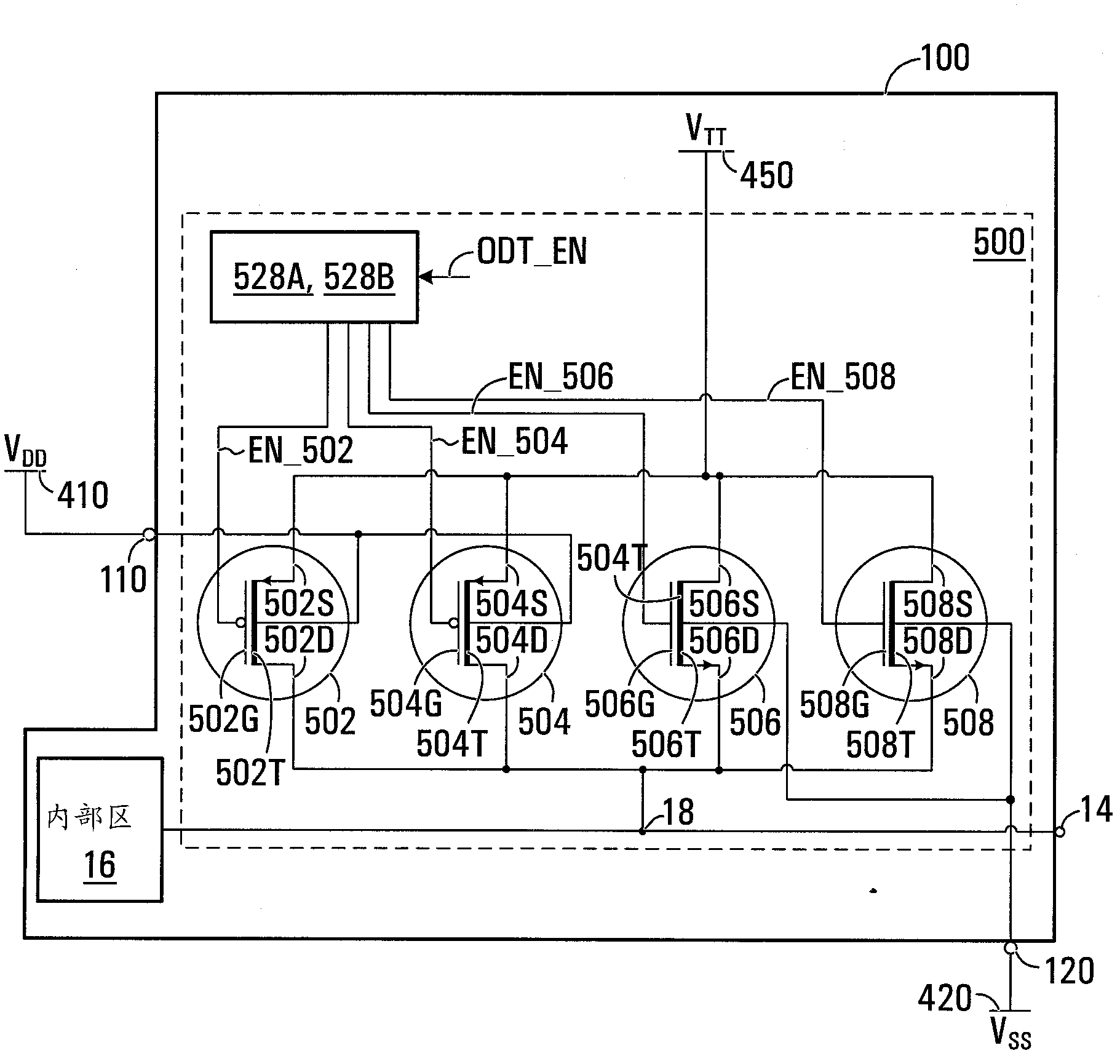
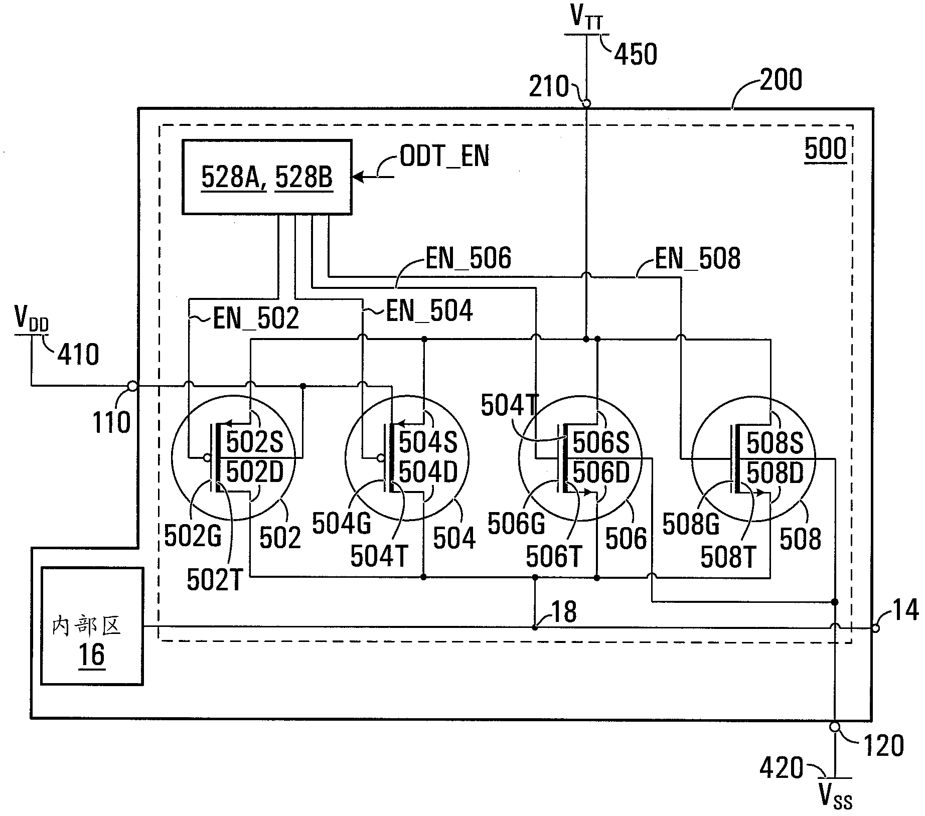
[0024] now refer to figure 1 with figure 2 , shows a termination circuit 500 for the on-chip termination of terminals 14 connected to the inner region 16 of the semiconductor device 100 , 200 . On-chip termination may be used to protect the integrity of signals transmitted and / or received via terminal 14 . Accordingly, the terminal 14 may be an input terminal, an output terminal or a bidirectional input / output terminal. In certain non-limiting embodiments, terminals 14 may be configured to transmit and / or receive data signals that vary between two voltage levels representing corresponding logic values. The semiconductor device 100, 200 including the internal region 16 and the terminal 14 may be a memory chip (such as dynamic random access memory (DRAM), synchronous DRAM (SDRAM), double data rate (DDR) SDRAM, etc.) or can benefit from chip Any other type of semiconductor device terminated within.
[0025] Although the termination circuit 500 is shown as being connected wi...
PUM
 Abstract
Description
Claims
Application Information