Array substrate and manufacturing method thereof, and liquid crystal display device

A liquid crystal display device and array substrate technology, which is applied in the manufacture of array substrates, array substrates and liquid crystal display devices, can solve problems such as disconnection, influence yield rate, defects, etc. low cost effect

Active Publication Date: 2012-04-04
TCL CHINA STAR OPTOELECTRONICS TECH CO LTD
View PDF6 Cites 4 Cited by
  • Summary
  • Abstract
  • Description
  • Claims
  • Application Information

AI Technical Summary

Problems solved by technology

In the existing array substrate, the line width of the data line will become smaller or even broken after the wet etching process, resulting in vertical broken lines or vertical line defects, affecting the yield rate

Method used


Image

  • Array substrate and manufacturing method thereof, and liquid crystal display device
  • Array substrate and manufacturing method thereof, and liquid crystal display device
  • Array substrate and manufacturing method thereof, and liquid crystal display device

Examples


Embodiment Construction

[0019] The present invention will be further described below in conjunction with the accompanying drawings and preferred embodiments.

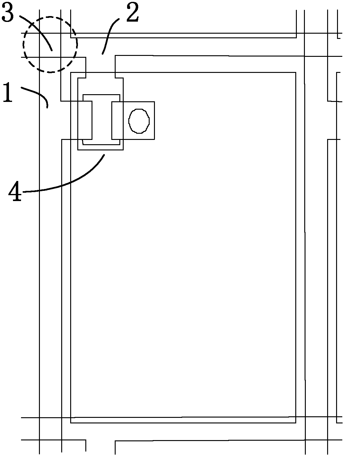
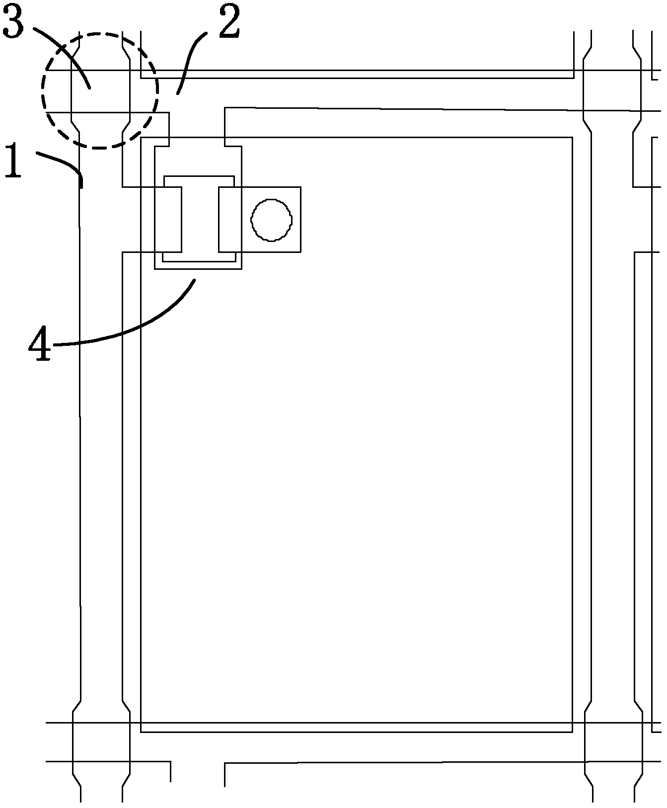
[0020] Such as image 3 As shown, a liquid crystal display device includes an array substrate, and the array substrate includes a plurality of thin film transistors 4, a scanning line 1 connected to the gates of the thin film transistors 4, a data line 2 connected to the sources of the thin film transistors 4, and the data lines 2 The width of the junction 3 of the data line 2 and the scan line 1 is greater than the width of the rest of the data line 2. Further, the widening width of the data line 2 on both sides of the junction 3 is equal. During the exposure and etching process, the intensity received by both sides of the data line 2 is equal, so the width of the widening is kept equal. After the exposure and etching process, the width of the data line 2 is uniform, and there will be no local narrowing or even disconnection.

[0021] Furth...


PUM


Abstract

The invention discloses an array substrate and a manufacturing method thereof, and a liquid crystal display device. The array substrate comprises a scanning line and a data line, wherein the width of the data line at the joint of the data line and the scanning line is greater than that of the other part of the data line. The invention has the advantages that: the yield of the liquid crystal display device can be improved on the premise of not increasing additional procedures; the process is simple; and the cost is low.

Description

technical field [0001] The present invention relates to the field of liquid crystal display, and more specifically, relates to an array substrate, a liquid crystal display device, and a manufacturing method of the array substrate. Background technique [0002] Existing array substrates are generally manufactured by etching process, and scanning lines and data lines are successively etched on the transparent substrate in layers, such as figure 1 , 2 As shown, the array substrate of the liquid crystal display device includes a plurality of thin film transistors (TFTs), and a thin film transistor includes a substrate, a gate and a source, the gate is connected to the scan line, and the source is connected to the data line. In the existing array substrate, the line width of the data lines will become smaller or even broken after the wet etching process, resulting in vertical broken lines or vertical line defects, which affects the yield rate. Contents of the invention [000...

Claims


Application Information

Patent Timeline
Patent Type & Authority Applications(China)
IPC IPC(8): G02F1/1362G02F1/1368H01L27/02H01L21/77
CPCG02F1/1368G02F1/1343G02F1/136286
Inventor 陈虹瑞
Owner TCL CHINA STAR OPTOELECTRONICS TECH CO LTD
Why Eureka
Try Eureka