Display panel device, and method for producing display panel device
A technology for display panels and substrates, used in identification devices, lighting devices, semiconductor/solid-state device manufacturing, etc. Instability, life shortening prevention, and power consumption reduction effects
- Summary
- Abstract
- Description
- Claims
- Application Information
AI Technical Summary
Problems solved by technology
Method used
Image
Examples
Embodiment approach 1
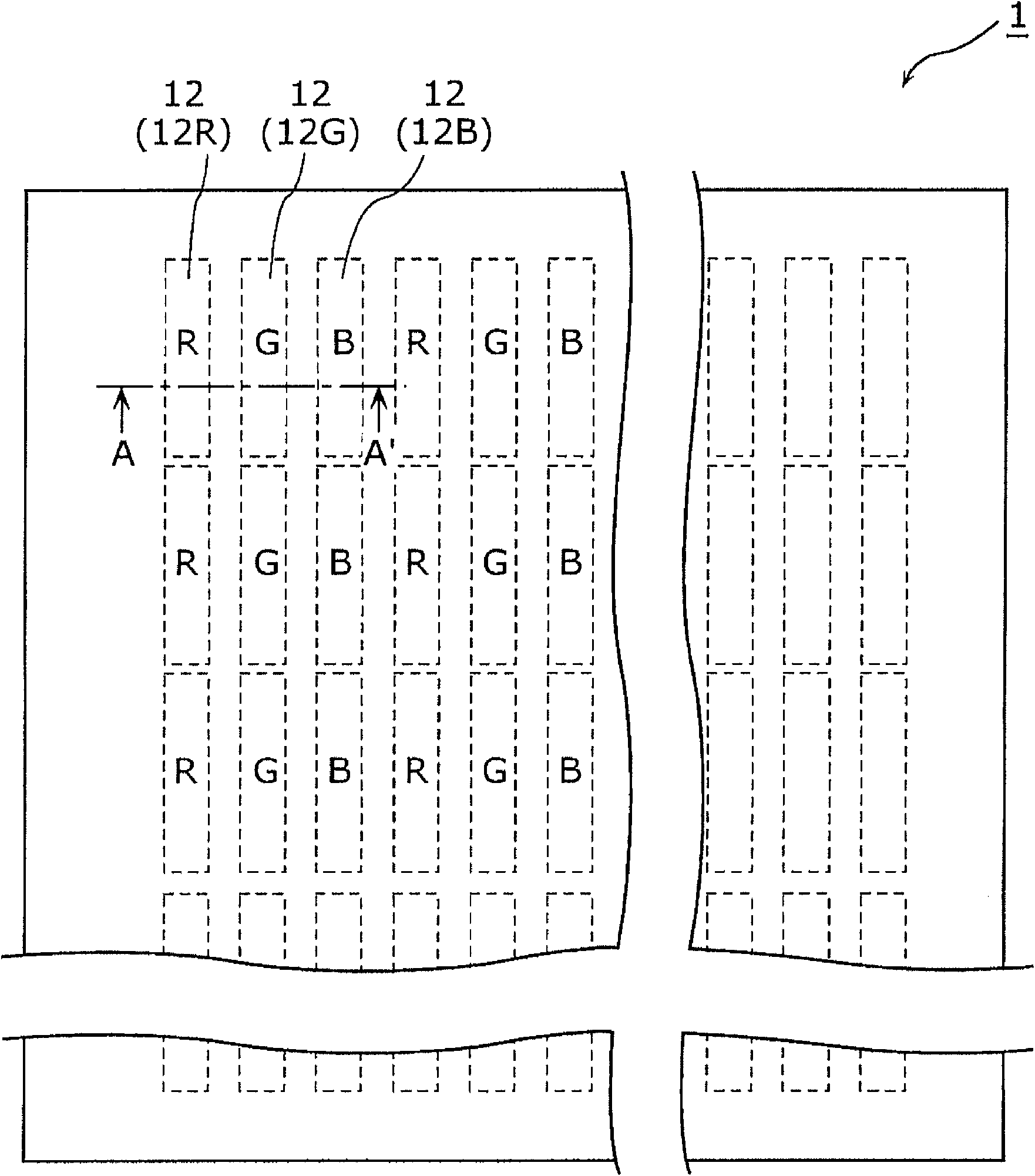
[0149] First, the display panel device 1 according to Embodiment 1 of the present invention will be described. figure 1 It is a plan view of the display panel device 1 according to Embodiment 1 of the present invention.
[0150] The display panel device 1 according to Embodiment 1 of the present invention includes a plurality of light emitting regions (not shown) formed in a row direction and a column direction perpendicular to the row direction (in a matrix). Multiple light emitting areas such as figure 1As shown, a light-emitting pixel portion (hereinafter, simply referred to as “pixel portion”) 12 is provided for each light-emitting region. Therefore, a plurality of pixel units 12 are arranged in a row direction and a column direction perpendicular to the row direction (in a matrix) for each light emitting region.
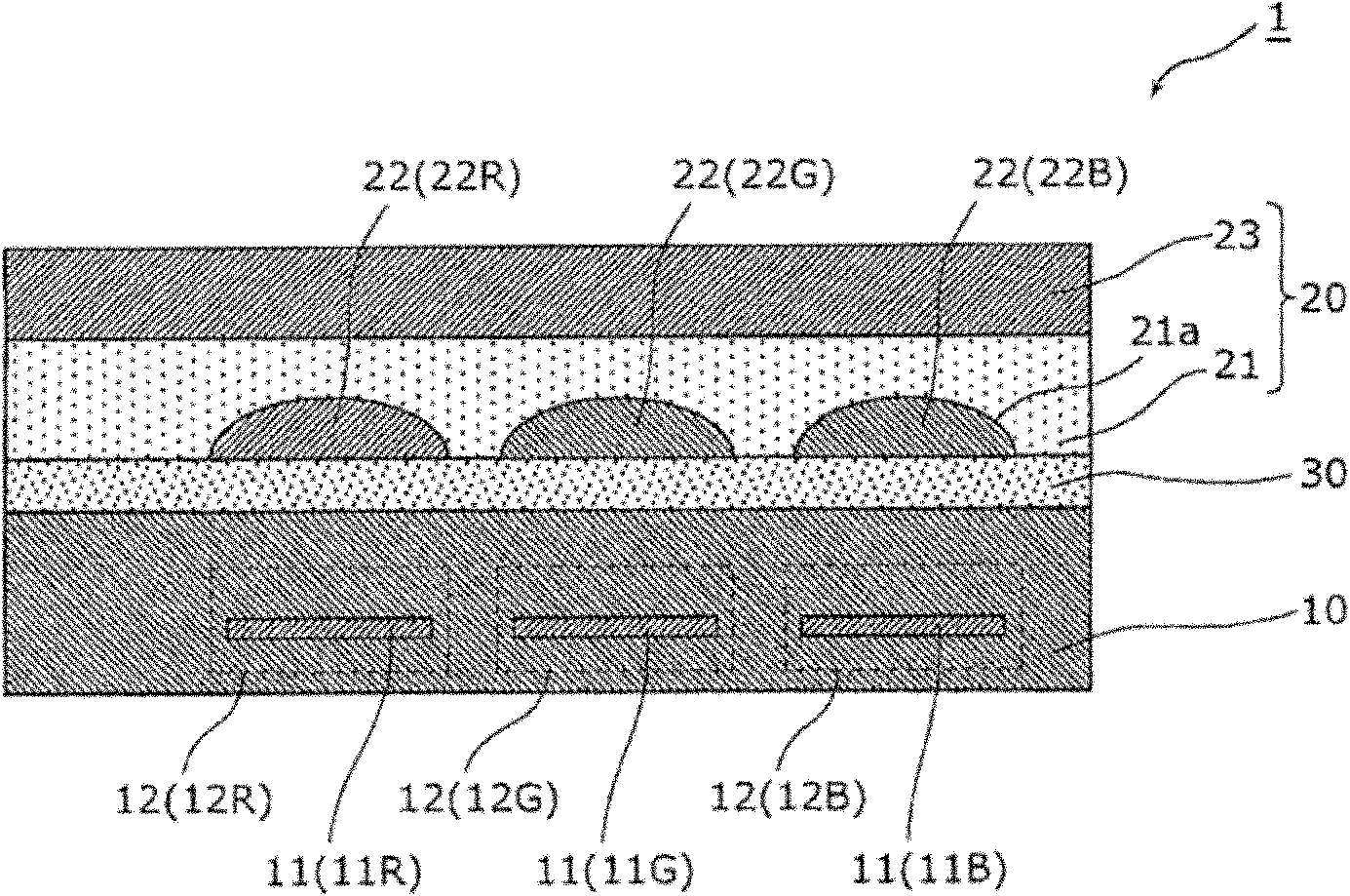
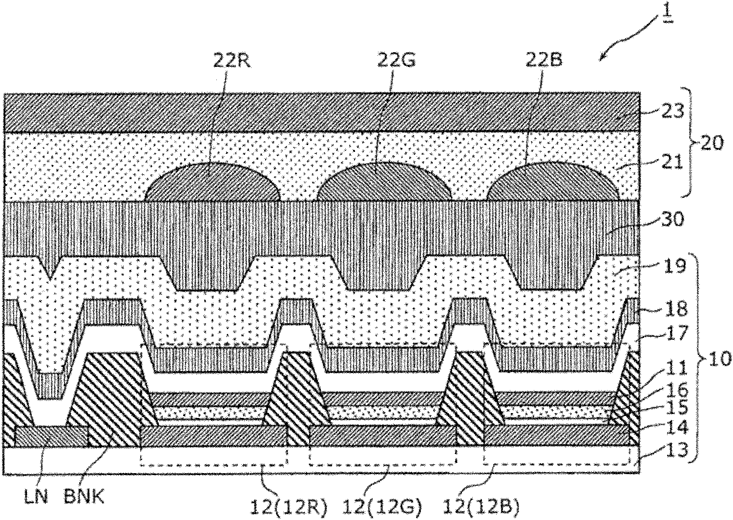
[0151] Each pixel unit 12 is connected to a pixel unit 12R that emits red light (hereinafter referred to as a “red pixel unit”), a pixel unit 12G that emits g...
Embodiment approach 2
[0202] Next, use Figure 8 A display panel device 2 according to Embodiment 2 of the present invention will be described. Figure 8 It is a partially enlarged cross-sectional view of the display panel device 2 according to Embodiment 2 of the present invention. In addition, in Figure 8 in, for with figure 2 The same configurations of the shown display panel device 1 according to Embodiment 1 of the present invention are assigned the same reference numerals, and description thereof will be omitted.
[0203] The display panel device 2 according to Embodiment 2 of the present invention is different from the display panel device 1 according to Embodiment 1 of the present invention in the structure of the resin layer and sealing resin.
[0204]In the display panel device 2 according to Embodiment 2 of the present invention, the resin layer 21B of the lens portion 20B has a convex portion 21 b protruding toward the organic EL portion 10 side. The convex portion 21b is formed t...
Embodiment approach 3
[0217] Next, use Figure 10 A display panel device 3 according to Embodiment 3 of the present invention will be described. Figure 10 It is a sectional view of the display panel device 3 according to Embodiment 3 of the present invention. In addition, in Figure 10 in, for with image 3 The same configurations of the shown display panel device 1 according to Embodiment 1 of the present invention are assigned the same reference numerals, and description thereof will be omitted.
[0218] In the display panel device 3 according to Embodiment 3 of the present invention, the resin layer 21C of the lens portion 20C has the second recessed portion 21c recessed toward the glass layer 23 side. The second concave portion 21c is formed between the concave portions 21a.
[0219] In the second concave portion 21c, the partition wall 24 is filled until the surface on the organic EL unit 10 side of the resin layer 21C becomes substantially flush with the surface. A light-absorbing mater...
PUM
 Abstract
Description
Claims
Application Information


