Plasma deposition source and method for depositing thin films

A plasma, deposition source technology, applied in the field of plasma-enhanced chemical vapor deposition system, which can solve the problems of reduced uptime and increased manufacturing costs of photovoltaic or microelectronic components

Inactive Publication Date: 2012-05-09
APPLIED MATERIALS INC
View PDF8 Cites 1 Cited by
  • Summary
  • Abstract
  • Description
  • Claims
  • Application Information

AI Technical Summary

Problems solved by technology

Alternatively, the manufacturing cost of photovoltaic or microelectronic components based on thin film deposition increases if the plasma deposition system has reduced uptime due to the formation of undesired exhaust gases

Method used


Image

  • Plasma deposition source and method for depositing thin films
  • Plasma deposition source and method for depositing thin films
  • Plasma deposition source and method for depositing thin films

Examples


Embodiment Construction

[0017] Various embodiments of the invention will now be described in detail with reference to one or more examples illustrated in the accompanying drawings. In the following description of the drawings, the same reference numerals refer to the same components. In general, only the differences of the various embodiments are described. Each example is provided by way of explanation of the invention, and each example is not meant to limit the invention. For example, features illustrated or described as part of one embodiment can be used on or in conjunction with other embodiments to yield yet a further embodiment. It is meant that the present invention includes the above-mentioned modifications and substitutions.

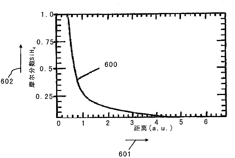
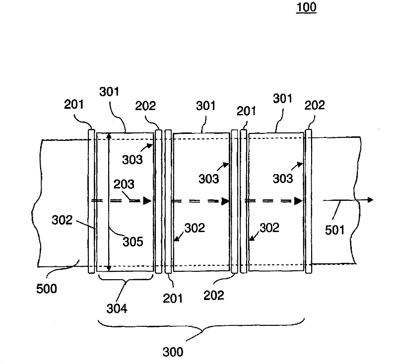
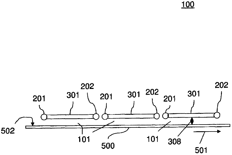
[0018] Embodiments described herein relate, inter alia, to plasma deposition systems for depositing thin films on moving substrates via the plasma phase. The substrate can be moved in a vacuum chamber along a substrate transport direction, wherein a plasma depositio...


PUM

PropertyMeasurementUnit
lengthaaaaaaaaaa
widthaaaaaaaaaa
lengthaaaaaaaaaa

Abstract

A plasma deposition source for transferring a deposition gas into a plasma phase and for depositing, from the plasma phase, a thin film onto a substrate moving in a substrate transport direction in a vacuum chamber is described. The plasma deposition source includes a multi-region electrode device adapted to be positioned in the vacuum chamber and including at least one RF electrode arranged opposite to the moving substrate, and an RF power generator adapted for supplying RF power to the RF electrode. The RF electrode has at least one gas inlet arranged at one edge of the RF electrode and at least one gas outlet arranged at the opposed edge of the RF electrode. A normalized plasma volume is provided by a plasma volume defined between an electrode surface and an opposite substrate position, divided by an electrode length. The normalized plasma volume is tuned to a depletion length of the deposition gas.

Description

technical field [0001] Embodiments of the invention relate to plasma enhanced chemical vapor deposition systems for depositing thin films on substrates. In particular, embodiments relate to plasma deposition sources that convert a deposition gas into a plasma phase via RF (radio frequency) electrodes. Furthermore, the invention relates to methods for depositing thin films on moving substrates. Background technique [0002] PECVD (Plasma Enhanced Chemical Vapor Deposition) provides a powerful tool to deposit thin films on various substrates. This type of thin film deposition has numerous applications in the microelectronics industry, for example, for depositing photovoltaic layers on flexible substrates, generally for modifying the surface of substrates, etc. Silicon-based deposition gases are used, for example, to prepare thinner silicon films on substrates for the manufacture of photovoltaic cells. Deposition gases used to deposit silicon-based materials on substrates ty...

Claims


Application Information

Patent Timeline
Patent Type & Authority Applications(China)
IPC IPC(8): H01J37/32
CPCC23C14/505H01J37/32H01J37/3277H01J37/32082
Inventor 尼尔·莫里森安德烈·赫佐格斯特凡·海因彼得·斯库克
Owner APPLIED MATERIALS INC
Why Eureka
Try Eureka