Seed Layers and Process of Manufacturing Seed Layers

a technology of manufacturing process and seed layer, applied in the field of seed layer, can solve the problems of low yield of seed layer, low quality of seed layer, and high defect rate of seed layer, and achieve the effect of reducing the cost per unit volume of cast crystalline silicon, high purity and high quality

Inactive Publication Date: 2010-08-05
AMG IDEAL CAST SOLAR
View PDF13 Cites 48 Cited by
  • Summary
  • Abstract
  • Description
  • Claims
  • Application Information

AI Technical Summary

Benefits of technology

[0008]This invention describes seed layers and relates a process of manufacturing seed layers for casting silicon suitable for use in solar cells or solar modules. Desirably, the process produces a high purity crystalline structure to create a robust high quality seed plate for use in silicon casting processes. This invention may include a process to produce seed layers corresponding in size to larger crucibles used for directional solidification. This invention may also include a process to produce monolithic seed layers that do not break during normal handling and can be used during several casting cycles. This invention may also include a process to lower the cost per unit volume of cast crystalline silicon by increasing a volume of cast silicon produced. The optimal application of the techniques disclosed here will result in defect-free or nearly defect-free seed crystals for large-area seeding.

Problems solved by technology

Without excessive care, loosely abutted seed tiles will tend to form highly defective crystal areas both in the fused seed layer and in the grown ingot above.
These highly defective areas grow and become problematic for the solar cells produced from the material, typically resulting in a lower solar cell efficiency.
The optimal application of the techniques disclosed here will result in defect-free or nearly defect-free seed crystals for large-area seeding.

Method used


Image

  • Seed Layers and Process of Manufacturing Seed Layers
  • Seed Layers and Process of Manufacturing Seed Layers
  • Seed Layers and Process of Manufacturing Seed Layers

Examples


Embodiment Construction

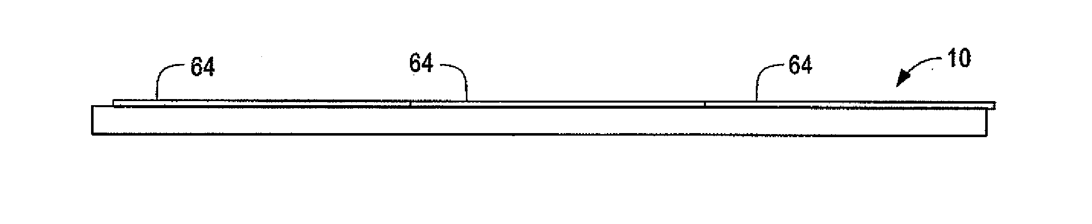
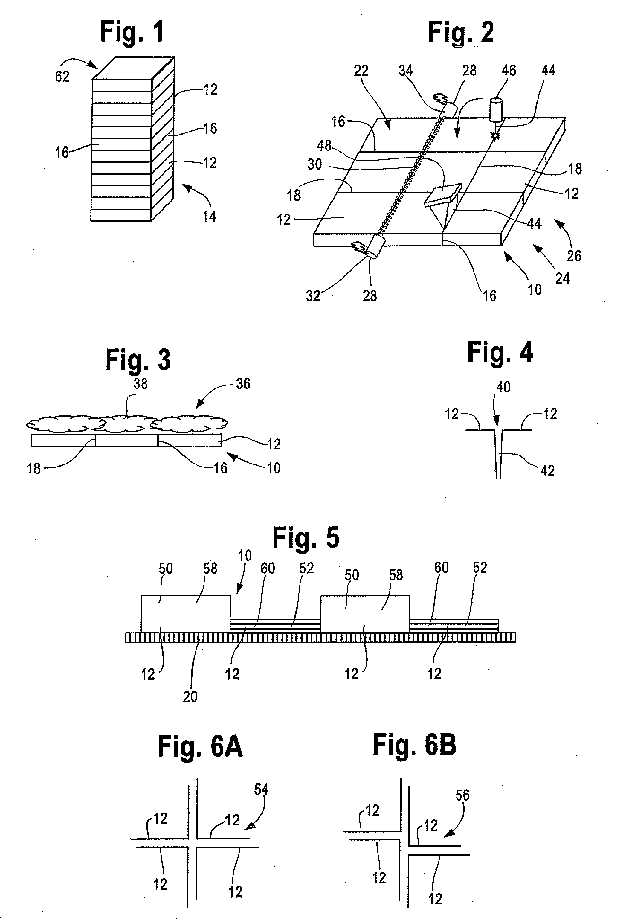
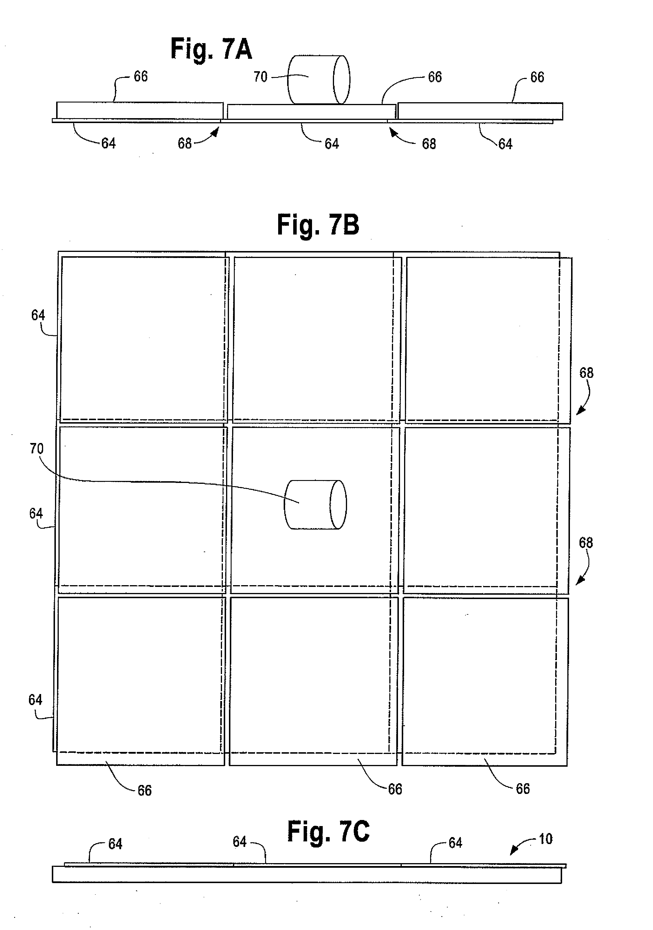
[0024]This invention describes seed layers and relates a process of manufacturing seed layers for casting silicon suitable for use in solar cells or solar modules. Directional solidification of silicon can allow the use of larger crucibles and larger scale manufacturing than known Czochralski or Float Zone techniques. Directional solidification may include using a seed crystal or seed layer to orient crystal growth, such as placing the seed layer on one more surfaces of the crucible or vessel. Accordingly, directional solidification can benefit from use of a very large single crystal seed layers. The seed layers can be any suitable size, such as at least about 500 millimeters squared, at least about 630 millimeters squared, at least about 750 millimeters squared, at least about 950 millimeters squared, and / or the like. Desirably, the seed crystal can be reused multiple times for several batches, such as by cutting the seed layer from the bottom of an ingot and placing the seed layer...


PUM

PropertyMeasurementUnit
temperatureaaaaaaaaaa
widthaaaaaaaaaa

Abstract

This invention relates seed layers and a process of manufacturing seed layers for casting silicon suitable for use in solar cells or solar modules. The process includes the step of positioning tiles with aligned edges to form seams on a suitable surface, and the step of joining the tiles at the seams to form a seed layer. The step of joining includes heating the tiles to melt at least a portion of the tiles, contacting the tiles at both ends of at least one seam with electrodes, using plasma deposition of amorphous silicon, applying photons to melt a portion of the tiles, and / or layer deposition. Seed layers of this invention include a rectilinear shape of at least about 500 millimeters in width and length.

Description

[0001]This application claims the benefit of priority from U.S. Provisional Patent Application 61 / 148,469, filed Jan. 30, 2009, the entirety of which is expressly incorporated herein by reference.BACKGROUND[0002]1. Technical Field[0003]This invention relates to seed layers and a process of manufacturing seed layers for casting silicon suitable for use in solar cells or solar modules.[0004]2. Discussion of Related Art[0005]Known steps to prepare seed material for silicon casting use a monocrystalline boule of silicon prepared by the Czochralski (CZ) technique or the float zone (FZ) technique. Both CZ and FZ techniques produce round or circular boules of material. The round boule is cut down to a square or rectangular cross-section and then sliced into pieces for the seed material. The conventional CZ and FZ techniques produce boules of up to a few hundred millimeters with very large boules being about 300-450 millimeters in diameter. Squaring the boule and slicing the seed material r...

Claims


Application Information

Patent Timeline
Patent Type & Authority Applications(United States)
IPC IPC(8): B28B7/36B29C65/02B29C65/16B29C65/14C30B25/02C30B25/20B32B38/10C01B33/02
CPCC30B11/14C30B29/06C30B28/06Y10T156/1043C30B1/023C30B33/04C30B33/06C30B28/04
Inventor STODDARD, NATHAN G.
Owner AMG IDEAL CAST SOLAR
Why Eureka
Try Eureka