Low-k spacer integration into CMOS transistors

a low-k spacer and transistor technology, applied in the field of low-k spacer integration into cmos transistors, can solve the problems of increasing the difficulty of making even smaller, and increasing the impediment of parasitic capacitance to good electrical performance, and carbon-silicon-oxide films tend to become much more conductiv

Inactive Publication Date: 2007-08-30
APPLIED MATERIALS INC
View PDF17 Cites 46 Cited by
  • Summary
  • Abstract
  • Description
  • Claims
  • Application Information

AI Technical Summary

Benefits of technology

[0005] Embodiments of the invention include methods of forming source and drain regions in a semiconductor transistor. The methods may include the step of forming a first sidewall spacer on sidewall surfaces of a gate electrode that is formed on an underlying substrate, where the first sidewall spacer comprises amorphous carbon. The methods may also include implanting the source and drain regions in the semiconductor substrate, and removing the first sidewall spacer before annealing the source and drain regions. The methods may further include forming a second sidewall spacer on the sidewall surfaces of the gate electrode, where the second sidewall spacer has a k-value less than 4.

Problems solved by technology

Each new generation of fabrication techniques and equipment are allowing commercial scale fabrication of ever smaller and faster transistors, but also increase the difficulty to make even smaller, faster circuit elements.
One increasing challenge to making smaller circuit elements is that as the elements get smaller, parasitic capacitance becomes an increasing impediment to good electrical performance.
Unfortunately, these carbon-silicon-oxide films tend to become much more conductive when exposed to temperatures (e.g., about 1000° C. or more) commonly used to anneal the source-drain and implant regions of a semiconductor transistor.
Another problem with substituting lower-k carbon-silicon-oxide materials for more conventional sidewall spacer materials is the reduced conformality seen in the deposition of these films.
Sidewall spacer depositions present conformality challenges not present with planar depositions on flat substrates.
The gate electrode is normally joined perpendicularly to the semiconductor substrate, making a high % conformality of the sidewall spacer difficult to achieve around the right angle junction of these elements.
The properties of carbon-silicon-oxide films make highly conformal depositions on the gate electrode sidewalls even more challenging.

Method used


Image

  • Low-k spacer integration into CMOS transistors
  • Low-k spacer integration into CMOS transistors
  • Low-k spacer integration into CMOS transistors

Examples


Embodiment Construction

Overview

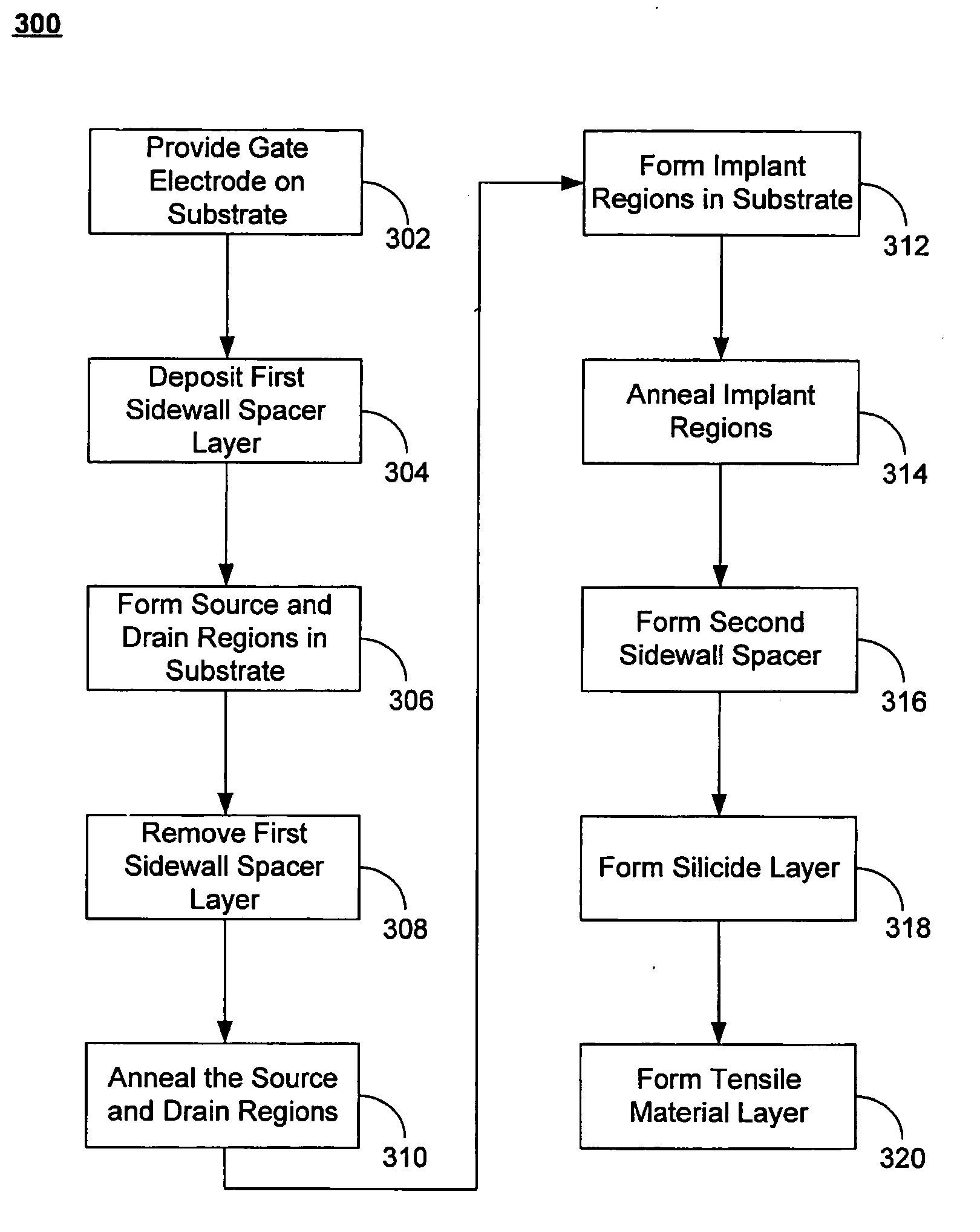
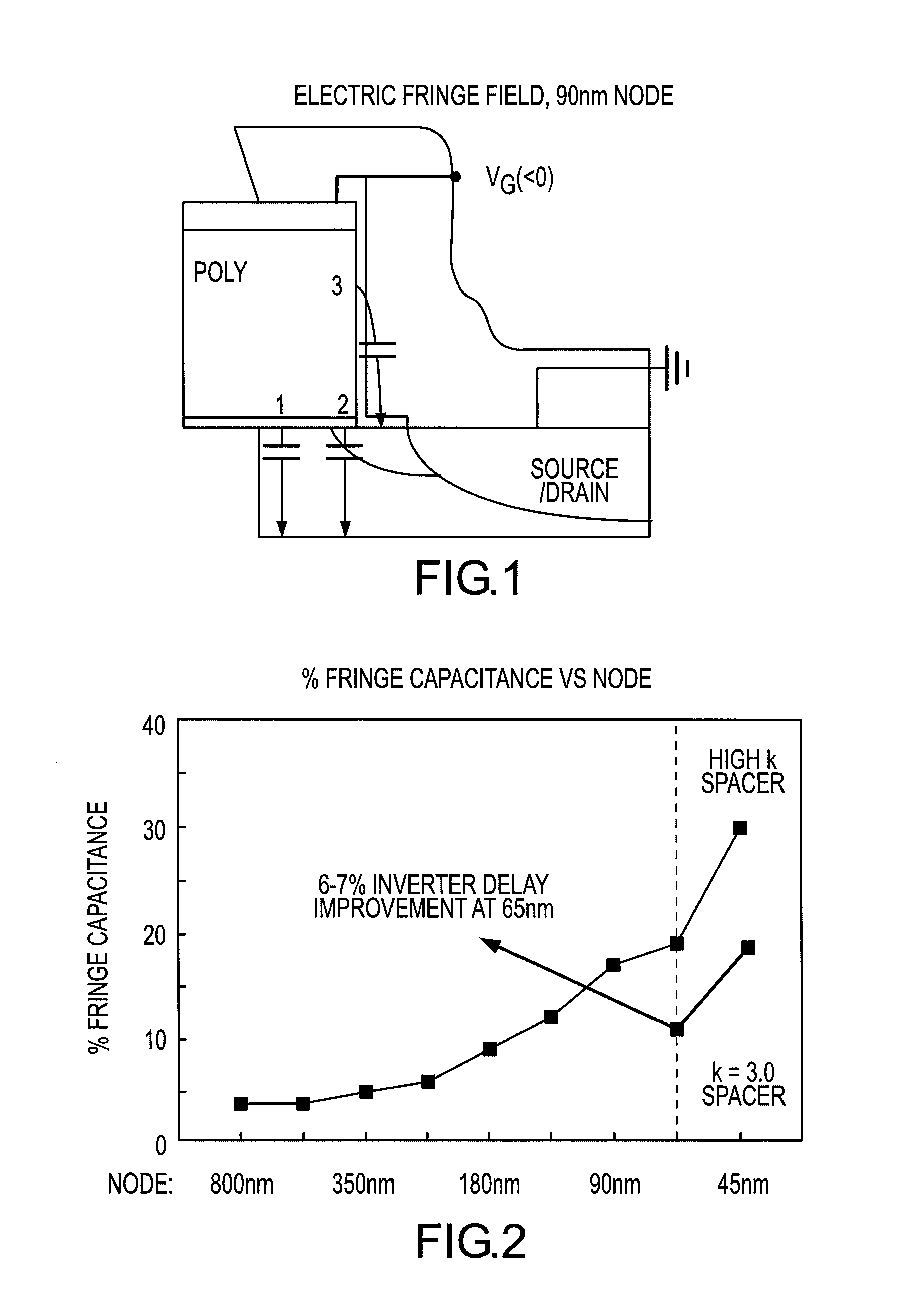
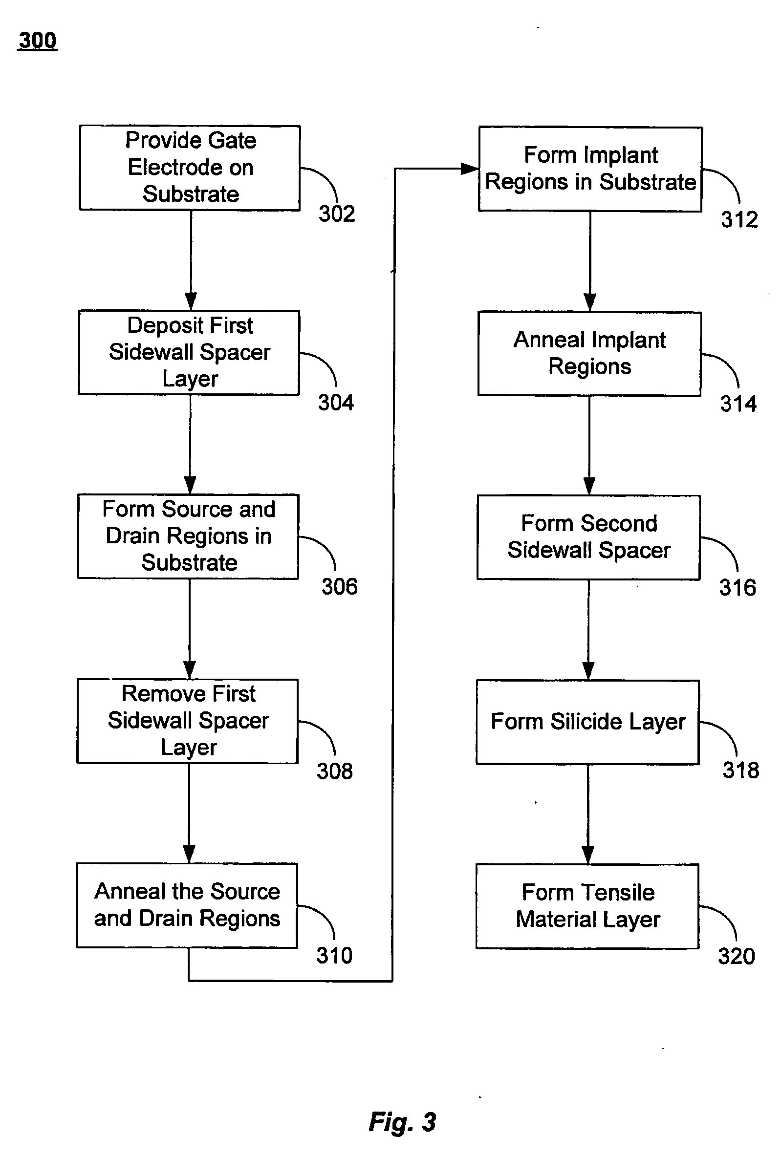
[0022] Systems and methods are described for forming conformal sidewall spacers that reduce the amount of fringe capacitance between the gate electrode and source / drain regions compared to conventional sidewall spacers with higher dielectric constants (i.e., k values). The methods include methods of forming low-k, carbon and silicon containing sidewall spacers after the formation and removal of a sacrificial spacer during the formation and high-temperature anneals (e.g., greater than 1000° C.) of the source / drain and other dopant regions, like halo regions, dopant extension regions, etc. The sacrificial spacer avoid the problem of the low-k spacer materials becoming conductive at high temperatures.

[0023] Also described are method of forming low-k spacers with improved conformality. Depositions of silicon and carbon containing spacer films often have reduced conformality when formed with conventional spacer deposition techniques (e.g., plasma deposition techniques for depo...


PUM


Abstract

A method of forming source and drain regions in a semiconductor transistor. The method includes the steps of forming a first sidewall spacer on sidewall surfaces of a gate electrode that is formed on an underlying substrate, where the first sidewall spacer includes amorphous carbon. The method may also include implanting the source and drain regions in the semiconductor substrate, and removing the first sidewall spacer before annealing the source and drain regions. The method may still further include forming a second sidewall spacer on the sidewall surfaces of the gate electrode, where the second sidewall spacer has a k-value less than 4. Also, a method to enhance conformality of a sidewall spacer layer. The method may include the steps of pulsing a radio-frequency power source to generate periodically a plasma, and depositing the plasma on sidewall surfaces of a gate electrode to form the sidewall spacer layer.

Description

BACKGROUND OF THE INVENTION [0001] Integrated circuit fabrication methods have reached a point where 50 to 100 million transistors or more are routinely formed on a single chip. Each new generation of fabrication techniques and equipment are allowing commercial scale fabrication of ever smaller and faster transistors, but also increase the difficulty to make even smaller, faster circuit elements. The shrinking dimensions of circuit elements, now well below the 100 nm threshold, has caused chip designers to look for new low-resistivity conductive materials and new low-dielectric constant (i.e., low-k) insulating materials just improve (and sometimes just to maintain) the electrical performance of the integrated circuit. [0002] One increasing challenge to making smaller circuit elements is that as the elements get smaller, parasitic capacitance becomes an increasing impediment to good electrical performance. As FIG. 1 shows, three components of parasitic capacitance associated with th...

Claims


Application Information

Patent Timeline
Patent Type & Authority Applications(United States)
IPC IPC(8): H01L21/338
CPCH01L21/02115H01L21/02126H01L21/0217H01L21/022H01L21/02216H01L21/02274H01L29/7843H01L21/26586H01L21/3146H01L21/31633H01L29/4983H01L29/665H01L29/6653H01L21/02362
Inventor AL-BAYATI, AMIRARGHAVANI, REZASHEK, MEI-YEEXIA, LI-QUNBALSEANU, MIHAELAKIM, BOK HOENCOX, MICHAEL S.PETERSON, CHADM'SAAD, HICHEM
Owner APPLIED MATERIALS INC
Why Eureka
Try Eureka