Packaging structure for ball grid array and manufacturing method for same

A packaging structure and ball grid array technology, applied in semiconductor/solid-state device manufacturing, semiconductor/solid-state device components, semiconductor devices, etc., can solve problems such as long time consumption, limited chip size, and complicated procedures, and achieve improved Efficiency, prevention of warpage, and reduction of cantilever effects

Active Publication Date: 2012-05-16
SAMSUNG SEMICON CHINA RES & DEV +1
View PDF4 Cites 44 Cited by
  • Summary
  • Abstract
  • Description
  • Claims
  • Application Information

AI Technical Summary

Problems solved by technology

[0007] 1) When the sizes of multiple chips are inconsistent and the size of the chip placed on the upper side is larger, a cantilever structure will be generated, which makes the wire bonding process more difficult, especially when the size of the cantilever protrudes is large , so this process is easily limited by the size of the chip;
[0008] 2) In the existing process, the first chip is first bonded to the substrate, then the first chip is subjected to a wire bonding process, and then the second chip is arranged on the upper side of the first chip, and then the The second chip performs the wire bonding process, so the process program needs to be carried out back and forth, the program is complicated, and the time consumed is relatively long;
[0009] 3) Since the chip is only arranged on one side of the substrate, the package structure is prone to structural warpage, especially when the overall size is thin

Method used


Image

  • Packaging structure for ball grid array and manufacturing method for same
  • Packaging structure for ball grid array and manufacturing method for same
  • Packaging structure for ball grid array and manufacturing method for same

Examples


Embodiment Construction

[0024] Hereinafter, a ball grid array package structure and a manufacturing method thereof according to embodiments of the present invention will be described in detail with reference to the accompanying drawings. However, the present invention can be implemented in many different ways and should not be construed as being limited to the following examples. In the drawings, the dimensions are exaggerated for clarity, and the same reference numerals are used in different drawings to designate the same components.

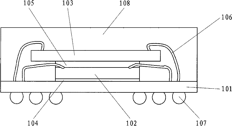
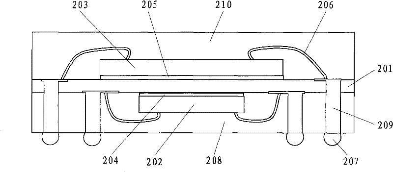
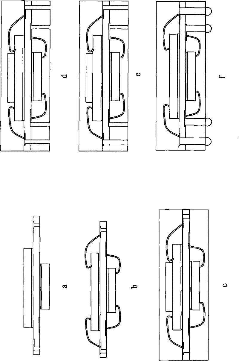
[0025] figure 2 It is a schematic diagram of a multi-chip packaging structure according to an embodiment of the present invention; image 3 It is a flowchart of a manufacturing process of the multi-chip packaging structure according to the present invention; Figure 4 It is a flowchart of another manufacturing process of the multi-chip package structure according to the present invention.

[0026] As can be seen from the figure, the multi-chip ball grid array pack...


PUM


Abstract

The invention relates to a packaging structure for a multi-chip ball grid array and a manufacturing method for the same, wherein the packaging structure for a ball grid array comprises a substrate; at least two chips fixed on the upper surface of the substrate and the lower surface of the substrate respectively, wherein a signal end is formed on each chip; pad parts disposed on the upper surface and the lower surface of the substrate and provided with through holes penetrating through the substrate in a thickness direction, wherein the pad parts form electric connections with the signal ends via leads; conducting parts which are conducting pins inserted and fixed in the through holes; and plastic packaging parts for protecting the substrate, the conducting parts and the chips. According to the packaging structure for a multi-chip ball grid array and the manufacturing method for the same disclosed by the invention, the generation for a cantilever in a multi-chip packaging can be reduced, the manufacturing technique can be simplified, and a warping phenomenon in structure can be prevented.

Description

technical field [0001] The present invention relates to a ball grid array packaging structure and a manufacturing method thereof, in particular to a ball grid array packaging structure and a packaging structure of a multilayer chip by arranging chips on the upper surface and the lower surface of a substrate and leading out an internal circuit through a conductive part. Manufacturing method. Background technique [0002] Ball grid array (BGA) packaging technology is a surface mount package that replaces traditional lead frames by making ball bumps in an array on the back of the substrate, making semiconductor devices more integrated. , better performance. BGA packaging technology will significantly increase the number of I / O pins of the device, reduce the pad pitch, and then reduce the size of the package and save the footprint of the package, so that the high density of PC chipsets, microprocessors, etc., Miniaturization of high-performance, multi-pin packaged devices is p...

Claims


Application Information

Patent Timeline
Patent Type & Authority Applications(China)
IPC IPC(8): H01L25/065H01L23/31H01L21/98
CPCH01L2924/15311H01L2224/32145H01L2224/73265H01L2224/48227H01L2224/32225H01L24/73H01L2924/00012
Inventor 汪民
Owner SAMSUNG SEMICON CHINA RES & DEV
Why Eureka
Try Eureka