Preparation method of physical detection sample

A technology for detecting samples and physics, applied in the preparation of test samples, semiconductor/solid-state device testing/measurement, electrical components, etc., can solve the problems of physical detection samples that are unfavorable to physical detection, and achieve the effect of improving reliability

Inactive Publication Date: 2012-05-23
SEMICON MFG INT (SHANGHAI) CORP +1
View PDF5 Cites 2 Cited by
  • Summary
  • Abstract
  • Description
  • Claims
  • Application Information

AI Technical Summary

Problems solved by technology

[0007] The object of the present invention is to provide a method for preparing a physical detection sample to solve the problem that the physical detection sample prepared by the existing physical detection sample preparation method is not conducive to physical detection

Method used


Image

  • Preparation method of physical detection sample
  • Preparation method of physical detection sample
  • Preparation method of physical detection sample

Examples


Embodiment Construction

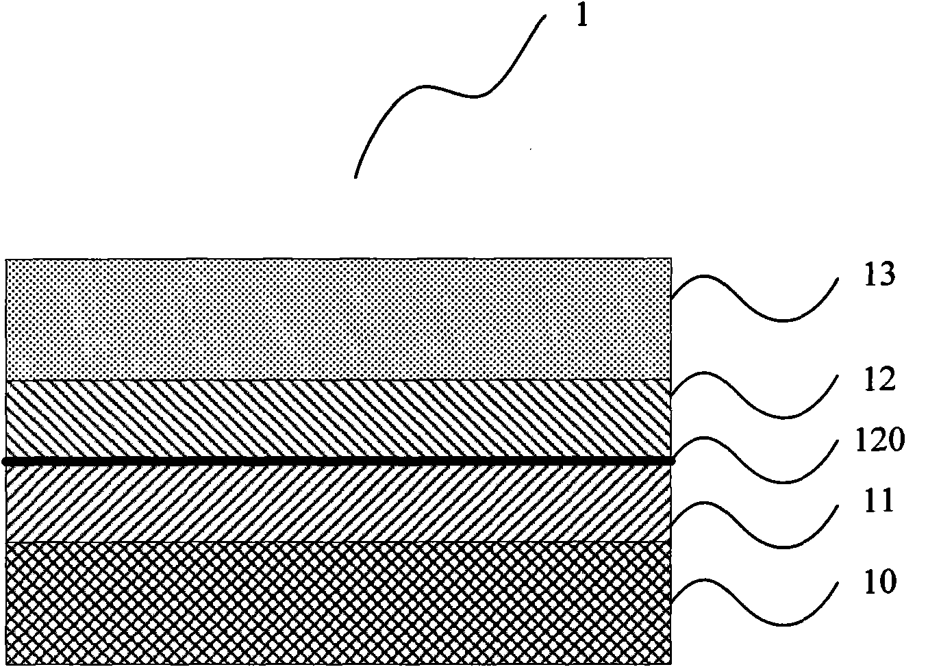
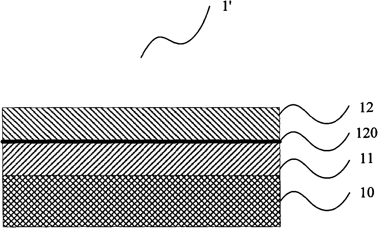
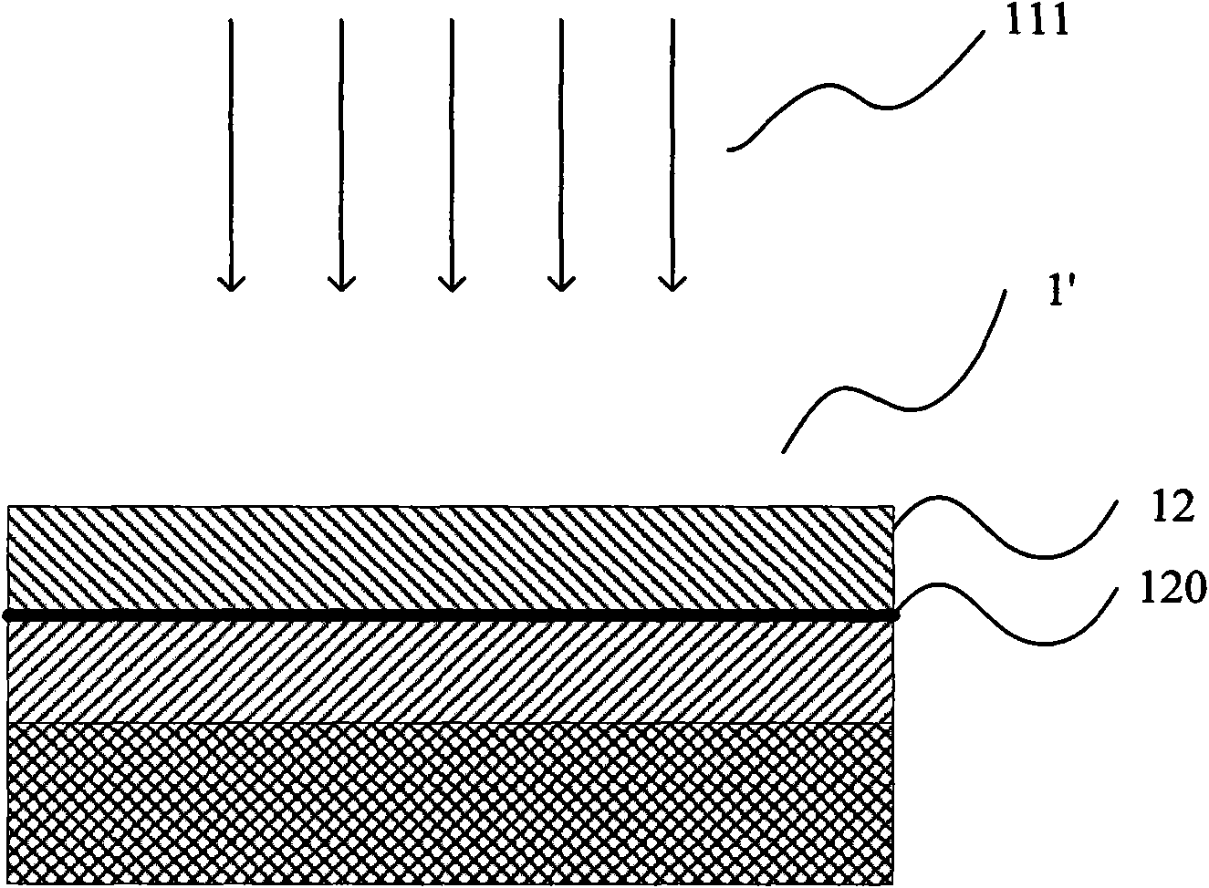
[0023] The physical detection sample preparation method proposed by the present invention will be further described in detail below in conjunction with the accompanying drawings and specific examples. Advantages and features of the present invention will be apparent from the following description and claims. It should be noted that all the drawings are in a very simplified form and use imprecise scales, and are only used to facilitate and clearly assist the purpose of illustrating the embodiments of the present invention.

[0024] The core idea of ​​the present invention is to provide a method for preparing a physical detection sample. The physical detection sample is prepared by peeling off the first physical layer in contact with the surface to be observed to expose the surface to be observed. In the physical detection sample thus prepared, the surface to be observed is exposed, that is, the surface to be observed is not blocked by any physical layer, and when the physical d...


PUM


Abstract

The invention provides a preparation method of a physical detection sample. The method comprises steps that: a wafer sectioned block is provided, wherein the wafer sectioned block comprises s first physical layer, a second physical layer and a third physical layer which grow sequentially, and a contact surface between the first physical layer and the second physical layer is a surface requiring observation; the first physical layer is stripped, such that the surface requiring observation is exposed, such that the physical detection sample is formed. With the method, the observation surface of the prepared physical detection sample is exposed, such that the observation surface is not obstructed by any physical layer. When the physical detection sample is observed by using a scanning electron microscope, the surface requiring observation can be clearly observed, such that the reliability of the physical detection can be improved.

Description

technical field [0001] The invention relates to an integrated circuit detection process, in particular to a method for preparing a physical detection sample. Background technique [0002] In the production of semiconductor devices, dozens or even hundreds of processes have to go through from the wafer to the final product. In order to ensure that the product has qualified performance, is stable and reliable, and has a high yield rate, according to the production situation of various products, there must be strict specific requirements for all process steps. Therefore, corresponding systems and precise monitoring measures must be established in the production process, starting from the semiconductor process inspection first. [0003] There are many items, contents and methods of semiconductor process testing, which can be roughly divided into two categories. The first category is the inspection of wafers before and after each step of processing or during processing, that is...

Claims


Application Information

Patent Timeline
Patent Type & Authority Applications(China)
IPC IPC(8): G01N1/28H01L23/544H01L21/66
Inventor 张佐兵高慧敏张顺勇林岱庆陈宏领
Owner SEMICON MFG INT (SHANGHAI) CORP
Why Eureka
Try Eureka