Phase change memory and manufacturing method thereof
A technology of phase change memory and manufacturing method, which is applied in the field of phase change memory and its manufacture, can solve the problems of high power consumption of phase change memory and failure to meet application requirements, and achieve the effect of reducing contact area and facilitating phase change
- Summary
- Abstract
- Description
- Claims
- Application Information
AI Technical Summary
Problems solved by technology
Method used
Image
Examples
Embodiment Construction
[0040] The power consumption of the phase change memory obtained by the existing manufacturing method is large, which cannot meet the requirements of the application. After research by the inventor, it is found that the reason for the large power consumption of the phase-change memory is that the phase-change current of the phase-change memory is relatively large. The reason for the large phase change current is that the contact area between the phase change layer of the phase change memory and the contact plug below is relatively large.
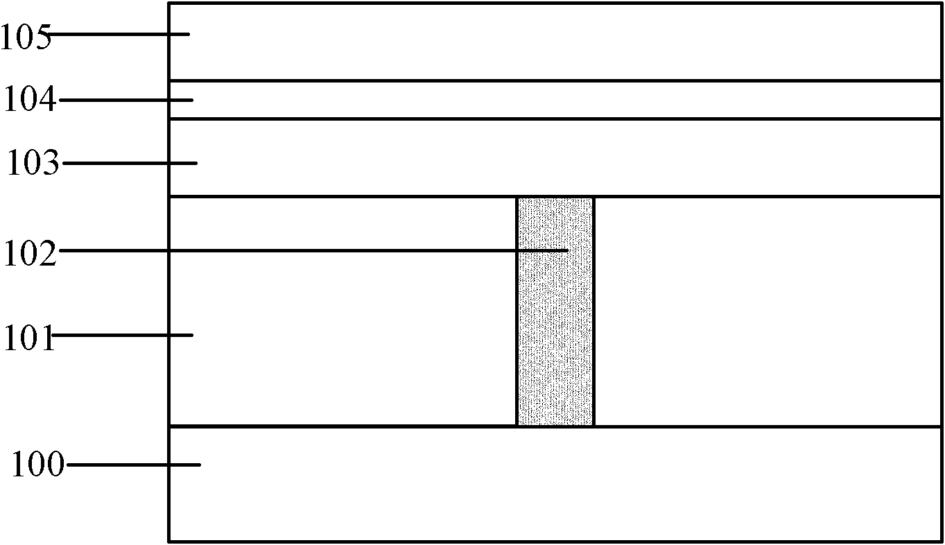
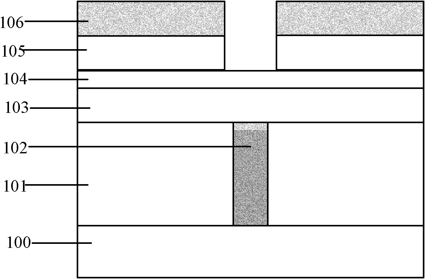
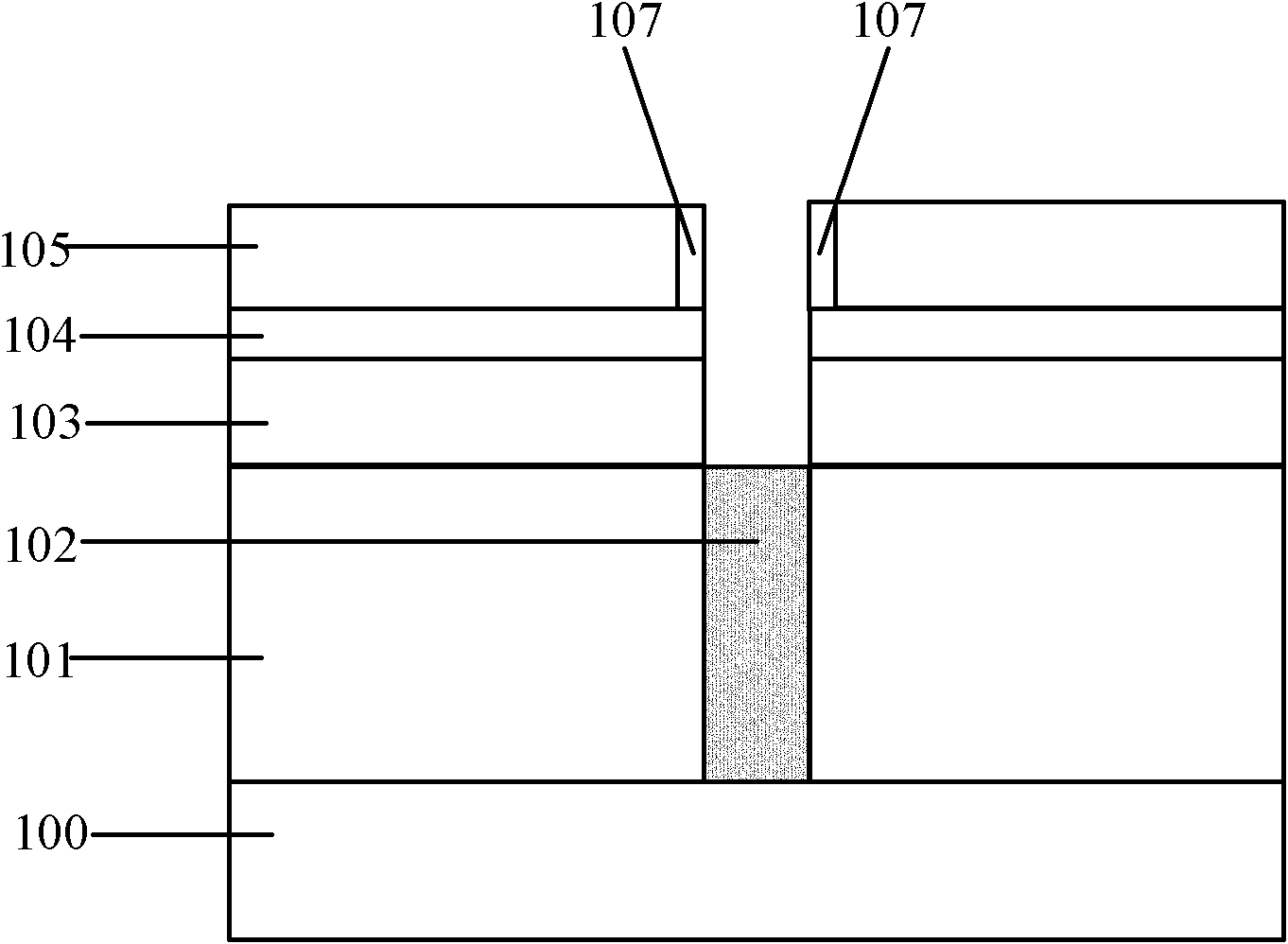
[0041] In order to solve the above problems, the present invention provides a manufacturing method of phase change memory, please refer to Figure 5 , is a schematic flow chart of the manufacturing method of the phase change memory of the present invention. The methods include:
[0042] Step S1, providing a semiconductor substrate, on which an interlayer dielectric layer and a contact plug located in the interlayer dielectric layer are for...
PUM
 Abstract
Description
Claims
Application Information


