Method for adjusting fin width in integrated circuitry

A fin and width technology, applied in the field of adjusting the width of fins in integrated circuits, can solve problems such as difficult control of contact landing process

Active Publication Date: 2012-05-30
TAIWAN SEMICON MFG CO LTD
View PDF9 Cites 7 Cited by
  • Summary
  • Abstract
  • Description
  • Claims
  • Application Information

AI Technical Summary

Problems solved by technology

Process control of contact landing becomes more difficult when horizontal and vertical gate lines coexist in multi-gate FinFET structures

Method used


Image

  • Method for adjusting fin width in integrated circuitry
  • Method for adjusting fin width in integrated circuitry
  • Method for adjusting fin width in integrated circuitry

Examples


Embodiment Construction

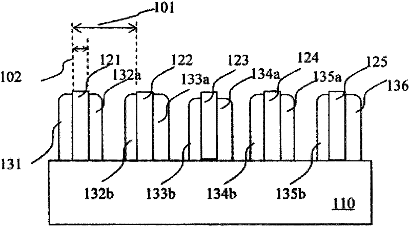
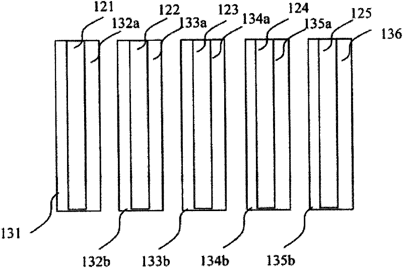
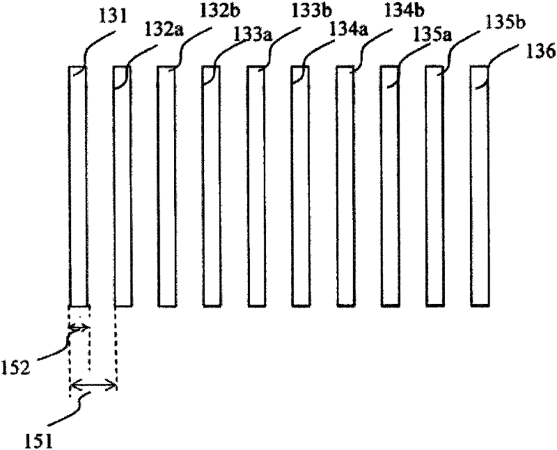
[0035]It is understood that the following description provides many different embodiments for implementing the various elements of the invention. Specific examples of components and arrangements are described below to simplify the present disclosure. These are of course merely examples and are not intended to be limiting. In addition, the following description in which a first component is formed on a second component may include an embodiment in which the first component and the second component are formed in direct contact, and may also include an embodiment in which an additional component is formed between the first component and the second component. Between embodiments such that the first and second components are not in direct contact. Various features may be arbitrarily drawn in different scales for clarity. In addition, the present invention may repeat reference numerals and / or letters in various instances. This repetition is for brevity only and does not in itself...


PUM


Abstract

A method includes growing a plurality of parallel mandrels on a surface of a semiconductor substrate, each mandrel has at least two laterally opposite sidewalls and a predetermined width. The method further includes forming a first type of spacers on the sidewalls of the mandrels, wherein the first type of spacers between two adjacent mandrels are separated by a gap. The predetermined mandrel width is adjusted to close the gap between the adjacent first type of spacers to form a second type of spacers. The mandrels are removed to form a first type of fins from the first type of spacers, and to form a second type of fins from spacers between two adjacent mandrels. The second type of fins are wider than the first type of fins.

Description

[0001] The present application is to a United States patent application for the following common application, which is hereby incorporated by reference in its entirety: U.S. Patent Application for "Method of Forming Metrology Structures from Fins in Integrated Circuits," filed November 19, 2010. Patent Application Serial No. 12 / 949,881 (Attorney Docket No. 24061.1573); and U.S. Patent Application Serial No. 12 / 952,376 (Attorney Docket No. No. 24061.1574). technical field [0002] The present invention relates to methods of adjusting the width of fins in integrated circuits. Background technique [0003] The present invention relates generally to semiconductor manufacturing and, more particularly, to integrated circuit devices and methods of forming these devices. [0004] The goals of the semiconductor industry remain higher density, higher performance, and lower cost. Scaling of device dimensions is the primary tool to achieve these goals. However, scaling beyond 100nm p...

Claims


Application Information

Patent Timeline
Patent Type & Authority Applications(China)
IPC IPC(8): H01L21/8234H01L21/762H01L21/336
CPCH01L21/845H01L27/1211H01L21/823431
Inventor 王建勋张智胜林以唐
Owner TAIWAN SEMICON MFG CO LTD
Why Eureka
Try Eureka