
Semiconductor device and manufacturing method thereof

A manufacturing method and semiconductor technology, applied in the direction of semiconductor/solid-state device manufacturing, semiconductor devices, electrical components, etc., can solve the problems of high consumption of Si, inability to withstand high annealing temperature of DRAM capacitors, harmful and other problems, and achieve the effect of high thermal stability

Active Publication Date: 2014-05-21
INST OF MICROELECTRONICS CHINESE ACAD OF SCI
View PDF4 Cites 0 Cited by
  • Summary
  • Abstract
  • Description
  • Claims
  • Application Information

AI Technical Summary

Problems solved by technology

[0007] 1. A very narrow gate (about 50nm) will lead to increased resistance (fine line width effect);
[0008] 2. A large amount of Si is consumed during the silicidation process, which is unbearable and harmful especially for the fabrication of devices with ultra-shallow junctions or on thin SOI substrates;
[0009] 3. Intrinsically rough CoSi 2 / Si interface will reduce the performance of the device;
[0018] All in all, silicide is widely used as source-drain contact in DRAM transistor manufacturing in order to reduce source-drain parasitic resistance and contact resistance, CoSi 2 Because the technology itself has some disadvantages and cannot continue to be used, people hope to use nickel-based silicide in this industry, but nickel-based silicide is usually not able to withstand the high annealing temperature of DRAM capacitors

Method used


Image

  • Semiconductor device and manufacturing method thereof
  • Semiconductor device and manufacturing method thereof
  • Semiconductor device and manufacturing method thereof

Examples


Embodiment Construction

[0034] The features and technical effects of the technical solutions of the present invention are described in detail below with reference to the accompanying drawings and schematic embodiments, and a novel DRAM device structure with thermally stable nickel-based silicide and a manufacturing method thereof are disclosed. It should be noted that similar reference numerals denote similar structures, and the terms "first", "second", "upper", "lower", etc. used in this application may be used to modify various device structures. These modifications do not imply a spatial, sequential, or hierarchical relationship of the modified device structures unless specifically stated.

[0035] The first example is Figures 3a to 5b As shown, a method for fabricating a thermally stable nickel-based silicide DRAM cell MOSFET with unraised source and drain regions is provided.

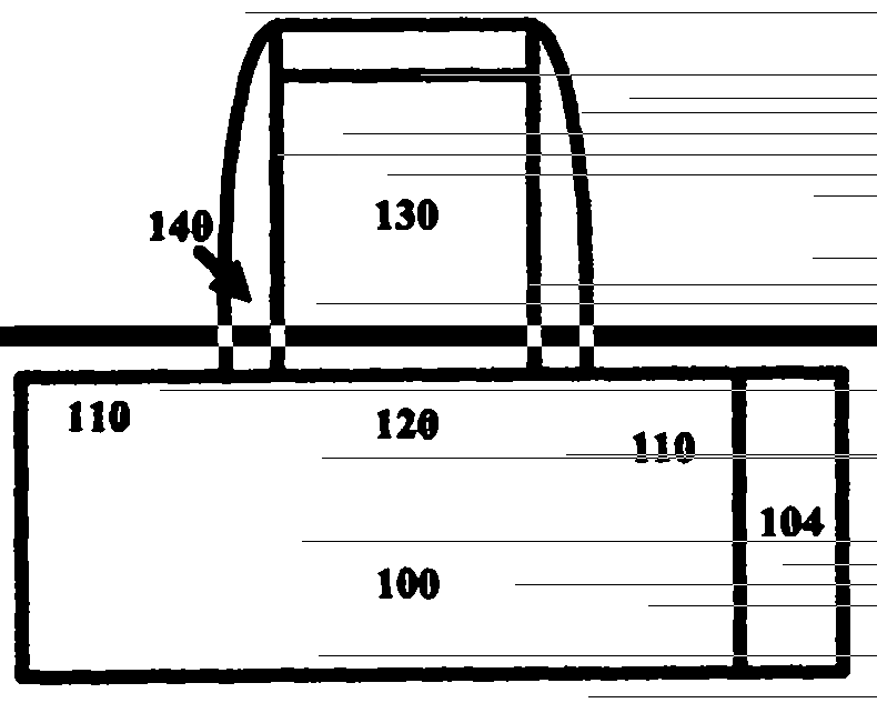
[0036] First, the basic structure of the MOSFET is formed. like Figure 3a As shown, a gate structure 130 is formed...


PUM

PropertyMeasurementUnit
thicknessaaaaaaaaaa
thicknessaaaaaaaaaa
thicknessaaaaaaaaaa

Abstract

The invention relates to a semiconductor device, comprising a substrate, a channel region and a source / drain region located in the substrate, a gate and a gate sidewall located on the channel region, and nickel-based silicide located on the source / drain region. The semiconductor device is characterized in that the nickel-based silicide is an epitaxial thin film layer. According to the invention, by reasonably setting the nickel-based silicide material and processing temperature, the nickel-based silicide can bear high-temperature annealing for eliminating capacitance defects of a DRAM (Dynamic Random Access Memory), thus the source / drain parasitic resistance and contact resistance of MOSFET (Metal-Oxide-Semiconductor Field-Effect Transistor) of the DRAM are lowered and the semiconductor device is compatible with the traditional CMOS manufacturing technique.

Description

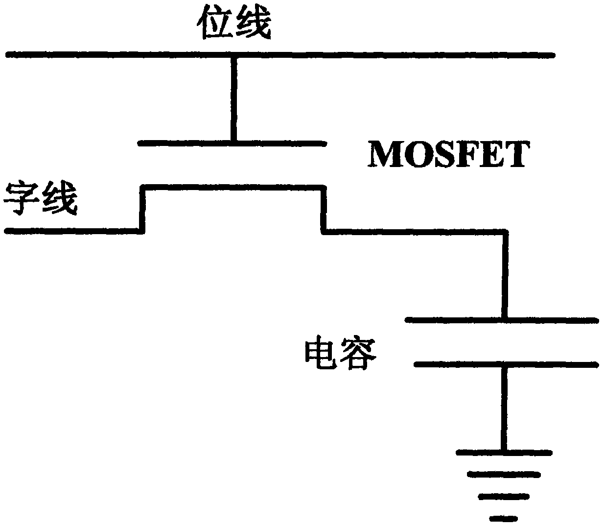
technical field [0001] The present invention relates to a semiconductor device and a manufacturing method thereof, in particular to a novel metal oxide semiconductor field effect transistor (MOSFET) structure with thermally stable nickel silicide and a manufacturing method thereof. Background technique [0002] MOS memory is a typical representative product of VLSI, which develops extremely rapidly and the products are constantly updated. The main product of MOS memory is random access memory (RAM), which is divided into static random access memory (SRAM) that stores information by bistable circuits, and dynamic random access memory (DRAM) that stores information by capacitors. [0003] As early as the mid-1970s, DRAM cells developed into a standard DRAM cell circuit form with a single-tube structure. like figure 1 Shown is the equivalent circuit of the single-tube unit. The single-tube unit is composed of a MOS tube and a capacitor (1T1C structure). The MOS tube plays the...

Claims


Application Information

Patent Timeline
Patent Type & Authority Patents(China)
IPC IPC(8): H01L29/78H01L29/45H01L21/336H01L21/28H01L21/283H01L21/324H01L21/8242
Inventor 罗军赵超
Owner INST OF MICROELECTRONICS CHINESE ACAD OF SCI
Learn More