Level shift circuit and semiconductor device

A technology of level shifting circuit and level, which is applied in the direction of electrical components, logic circuit connection/interface layout, logic circuit coupling/interface using field effect transistors, etc., and can solve the problem that the level shifting circuit 120 cannot operate normally.

Active Publication Date: 2012-05-30
CYPRESS SEMICON CORP
View PDF4 Cites 10 Cited by
  • Summary
  • Abstract
  • Description
  • Claims
  • Application Information

AI Technical Summary

Problems solved by technology

As a result, the level shifting circuit 120 may not function properly

Method used


Image

  • Level shift circuit and semiconductor device
  • Level shift circuit and semiconductor device
  • Level shift circuit and semiconductor device

Examples


Embodiment Construction

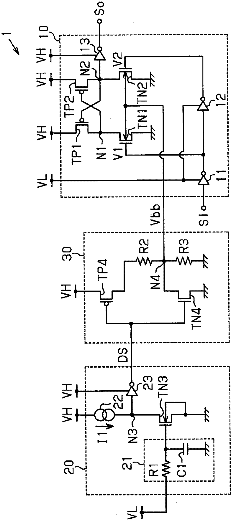
[0032] will now refer to Figure 1 to Figure 3 The first embodiment will be described.

[0033] The level shift circuit 1 converts the input signal Si having a signal level of a reference voltage (low potential voltage) and a first high potential voltage VL into a signal level having a reference voltage GND and a second high potential voltage VH (which is higher than the first high potential voltage) The output signal So of the signal level of the voltage VL). Hereinafter, for brevity, the level of the first high potential voltage VL is referred to as H1 level, the level of the second high potential voltage VH is referred to as H2 level, and the level of reference voltage GND is referred to as L level.

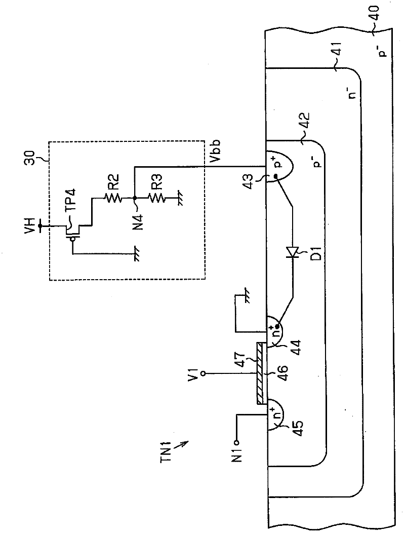
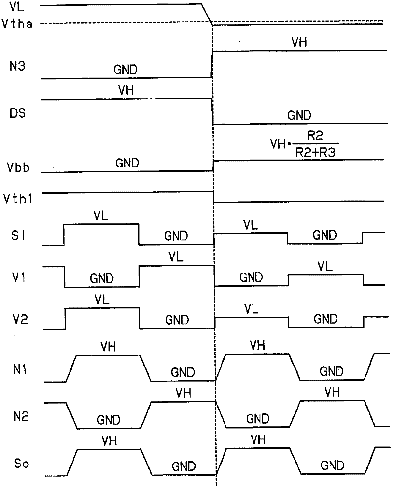
[0034] The level shifting circuit 1 includes a level conversion unit 10 , a detection unit 20 and a control unit 30 . The level converting unit 10 converts the input signal Si at the H1 level into the output signal So at the H2 level. The detection unit 20 detects a decrea...


PUM


Abstract

A level shift circuit including a level conversion unit that converts an input signal having a signal level of a first voltage into a signal having a signal level of a second voltage that is higher than the first voltage. The level conversion unit includes first and second MOS transistors of a first conductivity type and third and fourth MOS transistors of a second conductivity type, which differs from the first conductivity type and of which switching is controlled in accordance with the input signal. The third and fourth MOS transistors include drains supplied with the second voltage via the first and second MOS transistors, respectively. A control unit, when detecting a decrease in the first voltage, controls a body bias of the third and fourth MOS transistors to decrease a threshold voltage of the third and fourth MOS transistors.

Description

technical field [0001] The invention relates to a level shift circuit (level shift circuit) and a semiconductor device. Background technique [0002] Multi-power supply semiconductor large scale integration (LSI) includes a level shift circuit that interconnects circuits with different power supply voltages (for example, refer to Japanese Laid-Open Patent Publication No. 2005-252481, No. 05 -283997 and No. 06-204850). [0003] Figure 17 An example of a conventional level shifting circuit 120 is shown. [0004] The level shift circuit 120 outputs an output signal So corresponding to the input signal Si. The gate of the N-channel MOS transistor TN11 is supplied with an input signal Si having signal levels of the reference voltage GND and the first high potential voltage VL via the inverter circuit 121 . The gate of the N-channel MOS transistor TN12 is supplied with an input signal Si via an inverter circuit 121 and a further inverter circuit 122 . Therefore, the gates of ...

Claims


Application Information

Patent Timeline
Patent Type & Authority Applications(China)
IPC IPC(8): H03K19/0185
CPCH03K3/35613H03K2217/0018
Inventor 小川和树
Owner CYPRESS SEMICON CORP
Why Eureka
Try Eureka