Display device with optical data transmission

A technology for display devices and display substrates, applied to static indicators, instruments, etc., can solve problems such as visual non-uniformity, reduce production, etc., achieve the effects of tolerating lead wire and interconnector failures, increasing manufacturing costs, and reducing costs

Inactive Publication Date: 2012-05-30
GLOBAL OLED TECH
View PDF13 Cites 10 Cited by
  • Summary
  • Abstract
  • Description
  • Claims
  • Application Information

AI Technical Summary

Problems solved by technology

Positioning errors will cause visible non-uniformity and reduce yield

Method used


Image

  • Display device with optical data transmission
  • Display device with optical data transmission
  • Display device with optical data transmission

Examples


Embodiment Construction

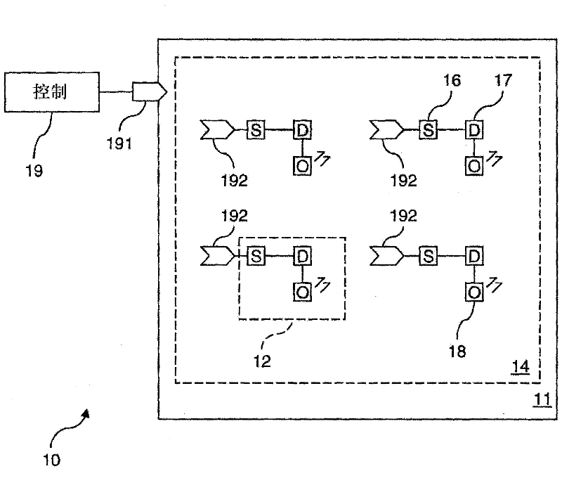
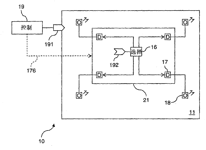
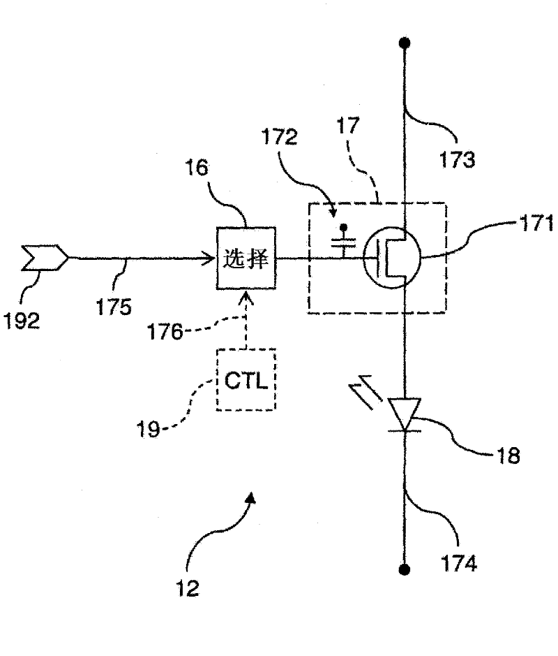
[0033] refer to Figure 1A A display device 10 according to an embodiment of the present invention includes a display substrate 11 on which a plurality of sub-pixels 12 are formed. Each sub-pixel 12 has a selection circuit 16 and a drive circuit 17 . Each subpixel 12 also includes display optics 18, such as electroluminescent (EL) emitters (light emitting elements). Each display optical element 18 is located in or above display area 14 and is responsive to drive circuitry to provide light. Connections within subpixels 12 may be accomplished electrically, optically, or by other means known in the art. Controller 19 provides pixel information to each selection circuit 16 to determine how much light is provided by each sub-pixel 12 .

[0034] The display substrate 11 defines an optical waveguide for transmitting light carrying pixel information. In this application, "light" when referring to pixel information includes all electromagnetic radiation (commonly referred to as "rad...


PUM


Abstract

A display device having a display substrate defining an optical waveguide for transporting light carrying pixel information; a chiplet disposed over the display substrate, having a chiplet substrate separate from the display substrate, a photosensor responsive to light from the optical waveguide at the selected control wavelength for providing the pixel information, a selection circuit responsive to the pixel information for providing a control signal, and a drive circuit responsive to the control signal, wherein the chiplet is adapted to receive the transported light; an optical transmitter for transmitting the pixel information from the controller as light at the selected control wavelength into the optical waveguide, and a display optical element located in or over the display area responsive to the drive circuit for providing light.

Description

[0001] Cross References to Related Applications [0002] This application is by reference to commonly assigned US Patent Application No. 12 / 480,804, filed June 9, 2009, entitled "Display Device with Parallel Data Distribution," to Cok et al. technical field [0003] The present invention relates to a display device having a substrate with distributed chiplets employing parallel control for an array of pixels. Background technique [0004] Flat panel display devices are widely used in conjunction with computer equipment, in portable equipment, and in entertainment equipment such as televisions. These displays typically display images using multiple pixels distributed over a substrate. The substrate is usually a continuous sheet of glass, but may also be plastic or other material, and may be divided into a plurality of adjacent pieces. Each pixel includes a number of differently colored light-emitting elements collectively called sub-pixels, typically emitting red, green, an...

Claims


Application Information

Patent Timeline
Patent Type & Authority Applications(China)
IPC IPC(8): G09G3/30G09G3/32
CPCG09G3/32G09G2370/18G09G3/2085G09G2360/141G09G2370/08G09G3/30
Inventor 克里斯多佛·J·怀特约翰·W·哈默
Owner GLOBAL OLED TECH
Why Eureka
Try Eureka