Resin plug-hole apparatus of PCB back borehole and method thereof

A technology of resin plugging and back drilling, which is applied in the direction of electrical connection formation of printed components, etc., and can solve problems such as many stepped through holes, large air bubbles, and poor reliability of circuit boards

Inactive Publication Date: 2012-06-27
SHENZHEN SUNTAK MULTILAYER PCB
View PDF3 Cites 43 Cited by
  • Summary
  • Abstract
  • Description
  • Claims
  • Application Information

AI Technical Summary

Problems solved by technology

[0005] For this reason, the object of the present invention is to provide a kind of resin plug hole device and method of PCB back drilling, to solve the current PCB back drilling for resin plug holes, there are more and larger air bubbles in the stepped through holes, resulting in The problem of poor reliability of the entire circuit board

Method used


Image

  • Resin plug-hole apparatus of PCB back borehole and method thereof
  • Resin plug-hole apparatus of PCB back borehole and method thereof
  • Resin plug-hole apparatus of PCB back borehole and method thereof

Examples


Embodiment Construction

[0020] To illustrate the idea and purpose of the present invention, the present invention will be further described below in conjunction with the accompanying drawings and specific embodiments.

[0021] The invention provides a resin plug hole device and method for PCB back drilling. It is mainly used in the production of some current PCB boards. Due to the stepped through holes, the resin ink is relatively sparsely combined in the hole during the resin plugging process. As a result, more and larger bubbles are generated in the stepped through holes, which leads to the problem of poor reliability of the entire circuit board.

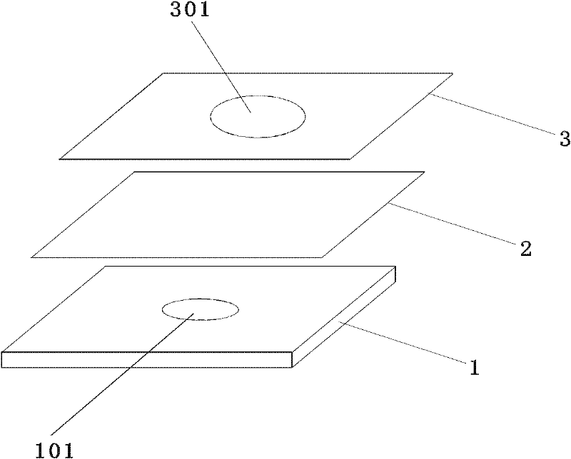
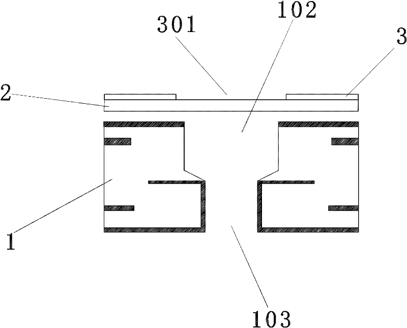
[0022] See figure 1 , figure 2 As shown, figure 1 It is a schematic diagram of the structure of the resin plug hole device for drilling the PCB back of the present invention; figure 2 for figure 1 Cutaway view. The resin plugging device for PCB back drilling of the present invention includes a PCB board 1, a screen printing screen 2 and an aluminum sheet 3....


PUM


Abstract

The invention discloses a resin plug-hole apparatus of a PCB back borehole and a method thereof. The apparatus comprises a PCB plate, a silkscreen net plate and an aluminum sheet. The PCB plate is drilled with a step through hole. One end of the step through hole is a back borehole with a large bore diameter, and the other end is a through hole with a small bore diameter. The silkscreen net plate is above one surface with the back borehole of the PCB back borehole and is provided with the aluminum sheet. According to the invention, the surface with the back borehole of the PCB plate is selected to be subjected to resin ink filling, resin ink flows through a larger hole and fills the step through hole, through controlling pressure, speed and times of scrapping, the step through hole is filled up by the resin ink, then the PCB plate is baked through a gradual temperature rise method, the resin ink in the hole is solidified, a volatile ingredient of the resin ink is discharged, a purpose of reducing bubbles in the step through hole is reached, and the reliability of a circuit board is raised.

Description

Technical field: [0001] The invention belongs to the technical field of PCB manufacturing, and specifically relates to a resin plug hole device and method for PCB back drilling. Background technique: [0002] In the PCB manufacturing process, through holes are needed to realize the connection between the inner layers. The through holes are usually formed by drilling machines, which require high processing accuracy. Moreover, after drilling through holes, they need to be processed by copper sinking and electroplating. , A conductive layer is formed in the through hole to realize the connection between the inner layers. However, the plated through holes of some PCB boards only need to be partially connected, and the through holes after the copper sinking and electroplating treatment are all connected Yes, this will cause the problem of the through-hole end connection, which will cause the signal to fold back, cause the signal transmission back reflection, scattering, delay and othe...

Claims


Application Information

Patent Timeline
Patent Type & Authority Applications(China)
IPC IPC(8): H05K3/40
Inventor 张军杰欧植夫刘东宋建远魏秀云
Owner SHENZHEN SUNTAK MULTILAYER PCB
Why Eureka
Try Eureka