
Method for burying and plugging holes on HDI (high-density interconnection) circuit boards

A circuit board and buried hole technology, applied in the field of circuit board manufacturing, can solve problems such as affecting PCB performance, and achieve the effects of improving efficiency, increasing surface roughness, and increasing bonding force

Active Publication Date: 2012-06-27
VICTORY GIANT TECH HUIZHOU CO LTD
View PDF7 Cites 7 Cited by
  • Summary
  • Abstract
  • Description
  • Claims
  • Application Information

AI Technical Summary

Problems solved by technology

[0005] The technical problem to be solved by the present invention is that in the existing HDI circuit board embedding hole technology, browning and lamination are generally arranged after the embedding hole is baked, because the embedded resin ink has a water absorption effect during browning and lamination. Problems that affect PCB performance, and provide a method for embedding holes on HDI circuit boards, including:

Method used


Image

  • Method for burying and plugging holes on HDI (high-density interconnection) circuit boards
  • Method for burying and plugging holes on HDI (high-density interconnection) circuit boards

Examples


Embodiment

[0044] The manual laminating machine and the screen printing machine described in this embodiment are all conventional equipment, and the screen plate used by the screen printing machine is an aluminum screen plate.

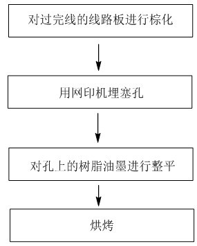
[0045] A method of plugging holes on a circuit board, comprising:

[0046] ①. The step of browning and pressing the HDI circuit board that has passed the line;

[0047] ②, the step of using the screen printing machine to bury the hole;

[0048] ③. The step of leveling the resin ink on the hole;

[0049] ④, the step of baking.

[0050] Among them, step ① can be operated according to the existing technology, and will not be described here. Step ② includes:

[0051] 1. Confirm whether the magnification of the aluminum stencil is consistent with that of the circuit board, and check whether the aluminum stencil meets the requirements (for example, whether there are burrs, pollutants, hole plugs, etc. on the surface of the aluminum stencil);

[0052] 2. Flatly set ...


PUM


Abstract

The invention belongs to the technical field of manufacturing circuit boards, relates to a burying and plugging process of HDI (high-density interconnection) circuit boards, in particular to a method for burying and plugging holes on the HDI circuit boards. The method for burying and plugging holes on the HDI circuit boards aims to solve the problems that brownification and press are generally performed after baking of buried and plugged holes in the existing process of burying and plugging holes on the HDI circuit boards so that performance of the PCBs is affected due to the fact that resin ink has a water absorption function during brownification and press, and includes: a, the brownification step of the HDI circuit boards distributed with wires; b, the step of hole burying and plugging by a screen printer; c, the process step of resin ink on the holes and d, the baking step. By the aid of the technical scheme, the above technical problems can be solved effectively.

Description

technical field [0001] The invention belongs to the technical field of circuit board manufacturing, and relates to a plugging process of an HDI circuit board, in particular to a method for embedding holes on an HDI circuit board. Background technique [0002] The plug hole at the back of the circuit board circuit is a method of HDI circuit board manufacturing process. The function of plugging is to prevent the phenomenon of glue shortage, depression and delamination of the board after lamination, reduce the risk of scrapping after lamination, and save time. ,save money. [0003] As an example, the process steps of the embedding method of the existing HDI circuit board are generally as follows: the plate after copper plating is directly plugged with a screen printer; the hole is baked after the plug is baked; after baking, the 6-axis grinder is used to grind 1- 2 times; make the circuit after grinding, and then press normally. [0004] That is to say, the browning and lamin...

Claims


Application Information

Patent Timeline
IPC IPC(8): H05K3/40
Inventor 龚俊邓松林张晃初
Owner VICTORY GIANT TECH HUIZHOU CO LTD
Learn More