

Method for processing monocrystal silicon carbide wafer
A wafer and machining allowance technology, which is used in metal processing equipment, stone processing equipment, fine working devices, etc., and can solve problems such as the inability to take into account the quality of the crystal surface.
- Summary
- Abstract
- Description
- Claims
- Application Information
AI Technical Summary
Problems solved by technology
Method used
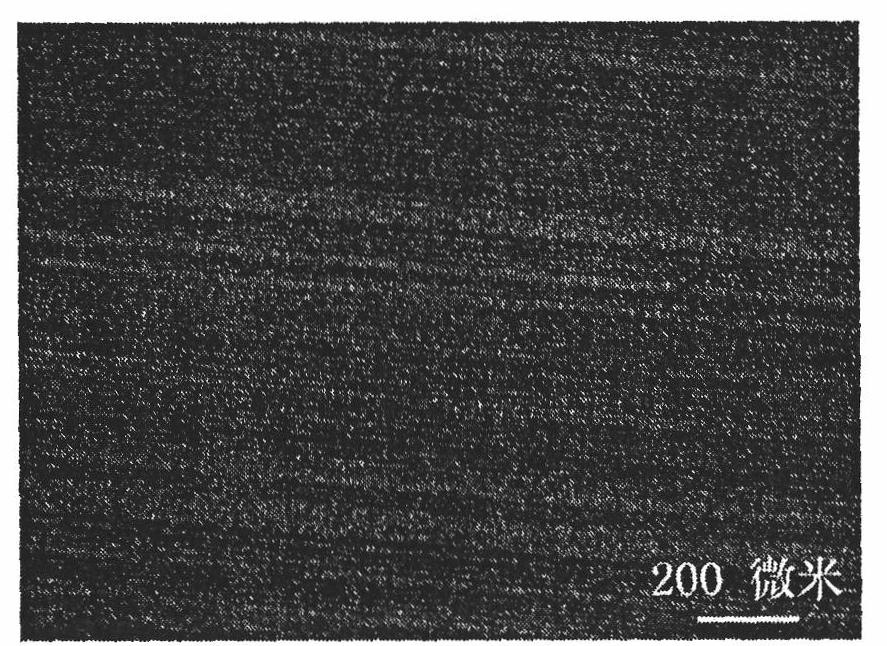
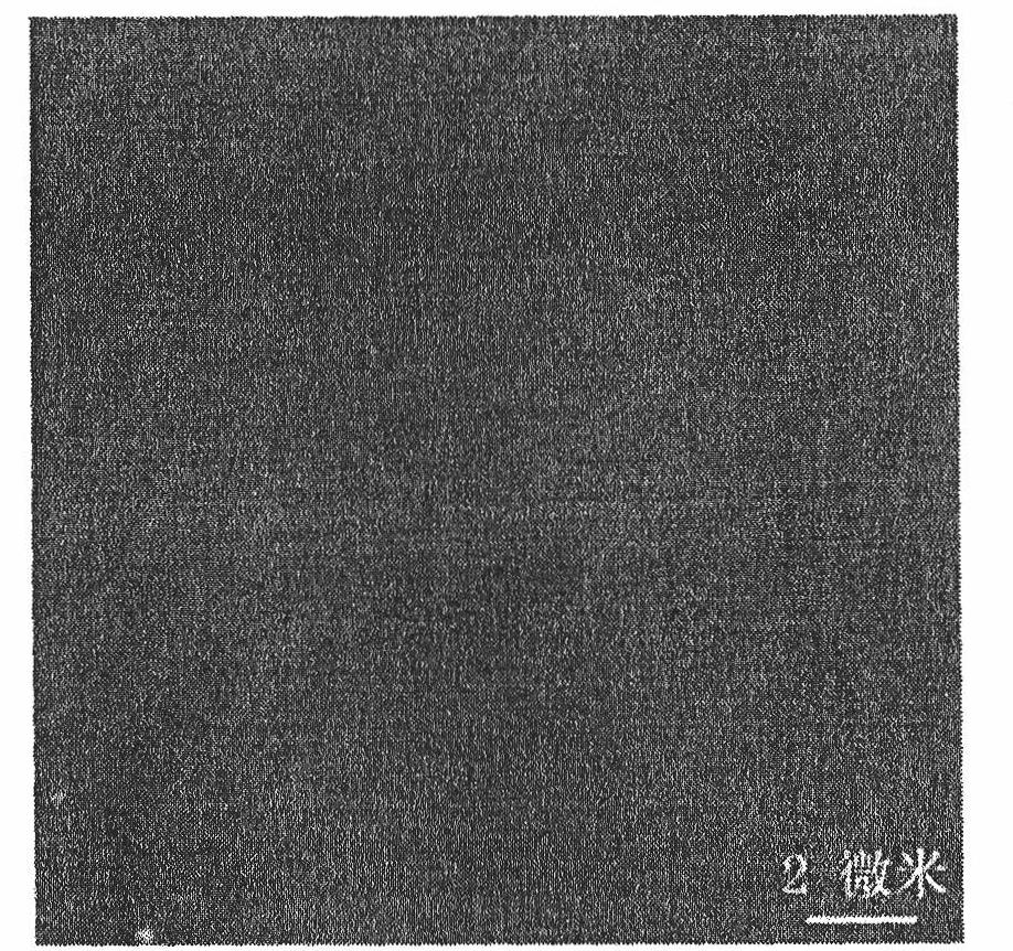
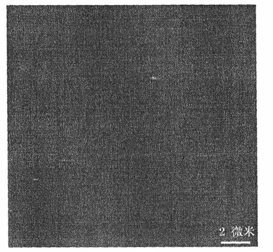
Image

Examples
Embodiment 1
[0042] Step 1: Take the 2-inch nitrogen-doped 4H-SiC single crystal wafer cut by wire cutting, and use SL-2 type cleaning agent to ultrasonically clean it for 10 minutes in 50Hz ultrasonic wave, and then ultrasonically clean it with absolute ethanol in 50Hz ultrasonic wave 10 minutes, set aside.
[0043] Step 2: Take the cleaned wafer, put it into the double-sided grinding machine, and adjust the pressure. The grinding pressure is 1 kg per piece with light pressure, 2 kg per piece with medium pressure, and 3 kg per piece with heavy pressure, and adjust each section. The number of grinding revolutions corresponding to the pressure is adjusted to 20 revolutions per minute of the grinding disc, and the flow rate of the grinding is adjusted to 30 milliliters per minute, and the grinding liquid is started to be processed. After the processing is completed, the removal amount is 15 microns, and the wafer is removed and cleaned in an ultrasonic wave with alcohol for 10 minutes, and t...
Embodiment 2
[0050] Step 1: Take the 2-inch nitrogen-doped 6H-SiC single crystal wafer cut by wire cutting, and use SL-2 type cleaning agent to ultrasonically clean it for 10 minutes in 50Hz ultrasonic wave, and then ultrasonically clean it with absolute ethanol in 50Hz ultrasonic wave 10 minutes, set aside.
[0051] Step 2: Take the cleaned wafer, put it into the double-sided grinding machine, and adjust the pressure. The grinding pressure is 1 kg per piece with light pressure, 2 kg per piece with medium pressure, and 3 kg per piece with heavy pressure, and adjust each section. The number of grinding revolutions corresponding to the pressure is adjusted to 90 revolutions per minute of the grinding disc, and the flow rate of the grinding is adjusted to 100 milliliters per minute, and the grinding liquid is started to be processed. After the processing is completed, the removal amount is 140 microns, and the chip is removed and cleaned in an ultrasonic wave with alcohol for 10 minutes, and ...
Embodiment 3
[0058] Step 1: Take the 2-inch semi-insulating 6H-SiC single crystal wafer cut by wire cutting, and use SL-2 type cleaning agent to ultrasonically clean it for 10 minutes in 50Hz ultrasonic wave, and then ultrasonically clean it with absolute ethanol in 50Hz ultrasonic wave 10 minutes, set aside.
[0059] Step 2: Take the cleaned wafer, put it into the double-sided grinding machine, and adjust the pressure. The grinding pressure is 1 kg per piece with light pressure, 2 kg per piece with medium pressure, and 3 kg per piece with heavy pressure, and adjust each section. The number of grinding revolutions corresponding to the pressure is adjusted to 50 revolutions per minute of the grinding disc, and the grinding flow rate is adjusted to 60 milliliters per minute, and the grinding liquid is started to be processed. After the processing is completed, the removal amount is 45 microns, and the chip is removed and cleaned in an ultrasonic wave with alcohol for 10 minutes, and then use...
PUM
| Property | Measurement | Unit |
|---|---|---|
| surface roughness | aaaaa | aaaaa |
| particle size | aaaaa | aaaaa |
Abstract
Description
Claims
Application Information