Polishing method for semiconductor wafer and polishing pad used therein

Inactive Publication Date: 2000-09-19
SHIN-ETSU HANDOTAI CO LTD
View PDF14 Cites 55 Cited by
  • Summary
  • Abstract
  • Description
  • Claims
  • Application Information

AI Technical Summary

Benefits of technology

When a silicon wafer is subjected to polishing, especially finish polishing, using the polishing

Problems solved by technology

Accordingly, while stable supply of wafers each with good surface roughness has become important, there is a fault in the above described polishing conditions that, when a polishing pad of a different production lot is used (when a polishing pad already in use is replaced with a new one still in the same polishing conditions), surface roughness of a wafer is sometimes det

Method used


Image

  • Polishing method for semiconductor wafer and polishing pad used therein
  • Polishing method for semiconductor wafer and polishing pad used therein
  • Polishing method for semiconductor wafer and polishing pad used therein

Examples


Example

Below, an preferred embodiment of the present invention will exemplarily be detailed in reference to the accompanying drawings. However, it is to be noted that dimensions and shapes of constituent parts described in the embodiment, relative positions thereof and the like are not intended to limit the scope of the present invention to the description of the embodiment unless otherwise specified, but the description should rather be construed for the purpose of illustration only.

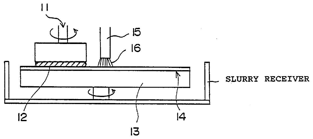
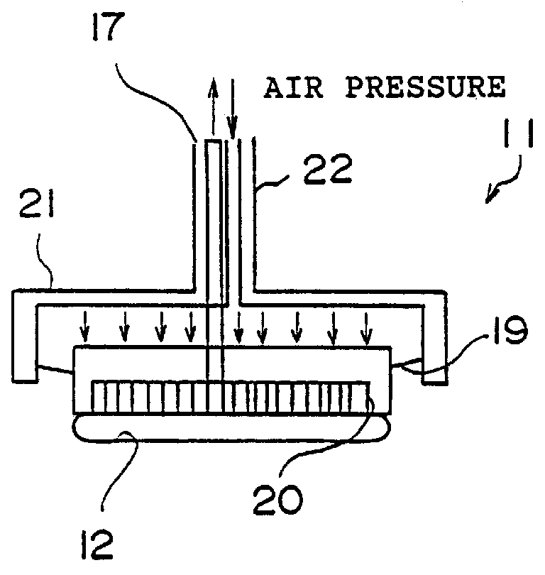
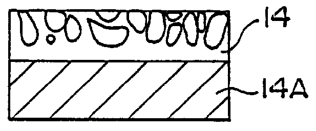
FIG. 1(A) shows an embodiment of a multi-staged wafer polishing method to which the present invention is applied and is a side elevational view showing an outline of a polishing apparatus. The polishing apparatus comprises: a polishing turn table 13 and a polishing head 11 which are respectively rotated in directions of arrows, wherein a polishing pad 14 is stuck on a polishing turn table 13, a wafer 12 is mounted in a polishing head 11, polishing slurry 16 in the state of slurry is supplied into a gap between...


PUM

PropertyMeasurementUnit
Currentaaaaaaaaaa
Surface roughnessaaaaaaaaaa

Abstract

In a polishing method for a semiconductor wafer in which polishing slurry is interposed between the semiconductor wafer and a polishing pad and the semiconductor wafer is mirror-polished by a polishing step for planarization, when polishing is conducted using a suede-like foam urethane resin polishing pad having physical properties of low compressibility lower than 9 % and high pore density equal to or higher than about 150 pores/cm.sup.2 as the polishing pad used in the polishing step, a mirror silicon wafer with good surface roughness of 50 bits in haze can be manufactured.

Description

BACKGROUND OF THE INVENTION1. Field of the InventionThe present invention relates to a polishing method for conducting mirror-polishing of a semiconductor wafer based on a mechano-chemical polishing method and particularly, to a polishing method for a semiconductor wafer in which the semiconductor wafer is mechano-chemically polished by a polishing step for planarization and improvement of surface roughness, wherein a polishing pad in the polishing step is improved and thereby micro-roughness, especially micro-roughness called haze is improved, and a polishing pad used in the polishing method.2. Description of the Prior ArtGenerally, a manufacturing process of a semiconductor wafer comprises a slicing step of slicing a single crystal ingot to obtain a thin disk like wafer, a chamfering step of chamfering the outer periphery of the wafer in order to prevent the wafer obtained in the slicing step from breakage or chipping, a lapping step of flattening the wafer, an etching step of rem...

Claims


Application Information

Patent Timeline
IPC IPC(8): B24B37/04B24D13/14B24D11/00B24D13/00B24D13/12B24B37/24
CPCB24B37/24
Inventor SUZUKI, KIYOSHIMASUMURA, HISASHIFUKAMI, TERUAKI
Owner SHIN-ETSU HANDOTAI CO LTD
Why Eureka
Try Eureka