Manufacturing method for electrochromic device and electrochromic device
A technology of electrochromic device and manufacturing method, which is applied in the directions of instruments, nonlinear optics, optics, etc., can solve the problems of poor generality of the manufacturing method, unsuitable for mass production, and high manufacturing cost, so as to reduce the manufacturing cost and improve the versatility. , Guaranteed quality effect
- Summary
- Abstract
- Description
- Claims
- Application Information
AI Technical Summary
Problems solved by technology
Method used
Image

Examples
Embodiment 1
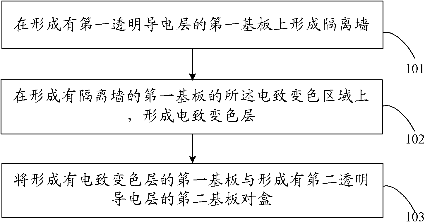
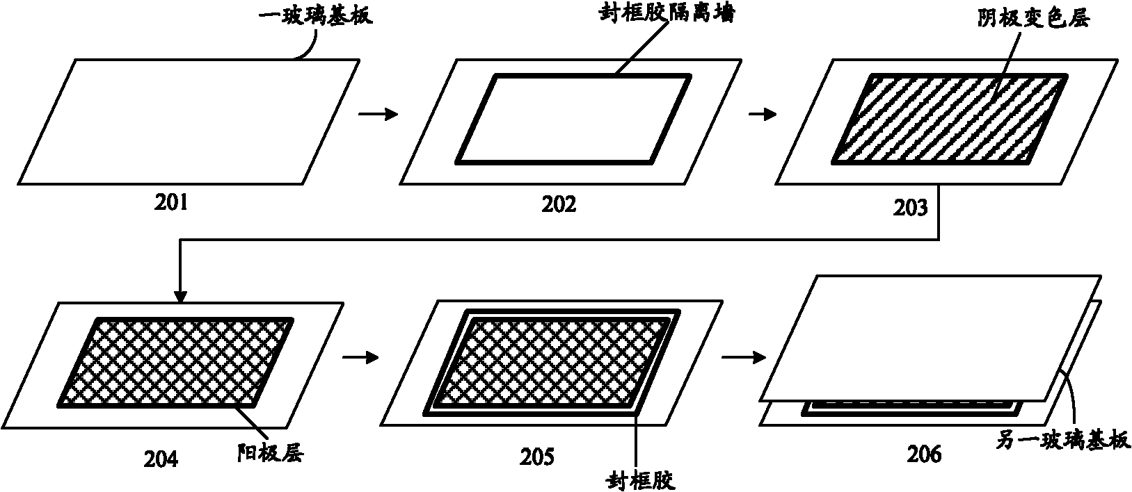
[0036] Such as image 3 As shown, this embodiment includes the following steps:
[0037] Step 201, providing a glass substrate formed with a first transparent conductive layer (first substrate formed with a first transparent conductive layer), and cleaning the glass substrate;
[0038] Step 202 , at a predetermined position on the glass substrate, a frame-sealing glue partition wall is formed by screen printing or a spreading process, and the frame-sealing glue partition wall is cured.
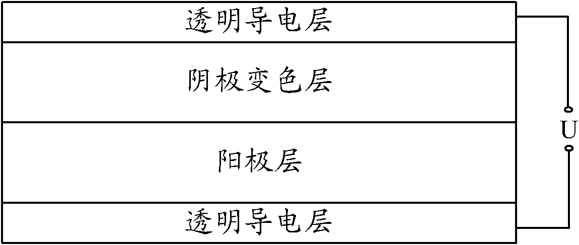
[0039] The frame sealing glue partition wall is a continuous partition wall, and the area surrounded by the frame sealing glue partition wall is the electrochromic region of the electrochromic device. In the subsequent steps, this region will form a cathode color-changing layer and an anode layer. For the electrochromic layer, since the instilled frame sealant includes components such as epoxy resin, catalyst and solution, in this step, the frame sealant partition wall is cured to prevent the...
Embodiment 2
[0051] The difference between the preparation method of this embodiment and the first embodiment lies in that the separation wall formed is different, such as Figure 4 As shown, this embodiment includes:
[0052] Step 301, providing a glass substrate formed with a first transparent conductive layer (first substrate formed with a first transparent conductive layer), and cleaning the glass substrate;
[0053] Step 302 , forming a photoresist isolation wall or a non-metal insulating isolation wall at a preset position on the glass substrate, and the area surrounded by the formed isolation wall is the electrochromic area of the electrochromic device.
[0054] When the isolation wall is a photoresist isolation wall, this step includes:
[0055] Coating photoresist on the glass substrate, exposing and developing through a mask plate, forming a photoresist isolation wall at a preset position on the glass substrate, and curing the formed photoresist isolation wall to prevent the i...
Embodiment 3
[0065] The preparation method of this embodiment, such as Figure 5 shown, including:
[0066] Step 401, providing a glass substrate formed with a first transparent conductive layer (first substrate formed with a first transparent conductive layer), and cleaning the glass substrate;
[0067] Step 402 , forming a photoresist isolation wall or a non-metal insulating isolation wall at a predetermined position on the glass substrate, and the area surrounded by the formed isolation wall is the electrochromic area of the electrochromic device.
[0068] Wherein, the partition wall is at least two partition walls arranged parallel to each other with discontinuities, and the at least two partition walls are complementary to each other, which can also achieve the effect of isolation and blocking.
[0069] Step 403 , forming a cathodic color-changing layer of the electrochromic layer on the glass substrate formed with the photoresist isolation wall or the non-metal insulating isolatio...
PUM
 Abstract
Description
Claims
Application Information
 - R&D
- Intellectual Property
- Life Sciences
- Materials
- Tech Scout
- Unparalleled Data Quality
- Higher Quality Content
- 60% Fewer Hallucinations
Browse by: Latest US Patents, China's latest patents, Technical Efficacy Thesaurus, Application Domain, Technology Topic, Popular Technical Reports.
© 2025 PatSnap. All rights reserved.Legal|Privacy policy|Modern Slavery Act Transparency Statement|Sitemap|About US| Contact US: help@patsnap.com