Method of manufacturing wiring substrate and method of manufacturing electronic component mounting structure

a technology of mounting structure and wiring substrate, which is applied in the direction of printed circuit manufacturing, printed circuit aspects, conductive pattern formation, etc., can solve the problem that the method is not always reliabl

Active Publication Date: 2007-06-07
SHINKO ELECTRIC IND CO LTD
View PDF7 Cites 29 Cited by
  • Summary
  • Abstract
  • Description
  • Claims
  • Application Information

AI Technical Summary

Benefits of technology

[0019] As described above, according to the present invention, it is possible to manufacture a wiring substrate which has no a core substrate without generating any troubles.

Problems solved by technology

However, in the above-described manufacturing methods in the prior art, in many case, wrinkles may occur in the build-up wiring layer in a series of steps of forming the build-up wiring layer on the temporary substrate in the detachable state, by virtue of heat stress applied in heating steps in the manufacturing processes, the heat stress due to differences between the thermal expansion coefficients in the structures.
Accordingly, these methods are not always sufficient in reliability.

Method used


Image

  • Method of manufacturing wiring substrate and method of manufacturing electronic component mounting structure
  • Method of manufacturing wiring substrate and method of manufacturing electronic component mounting structure
  • Method of manufacturing wiring substrate and method of manufacturing electronic component mounting structure

Examples


first embodiment

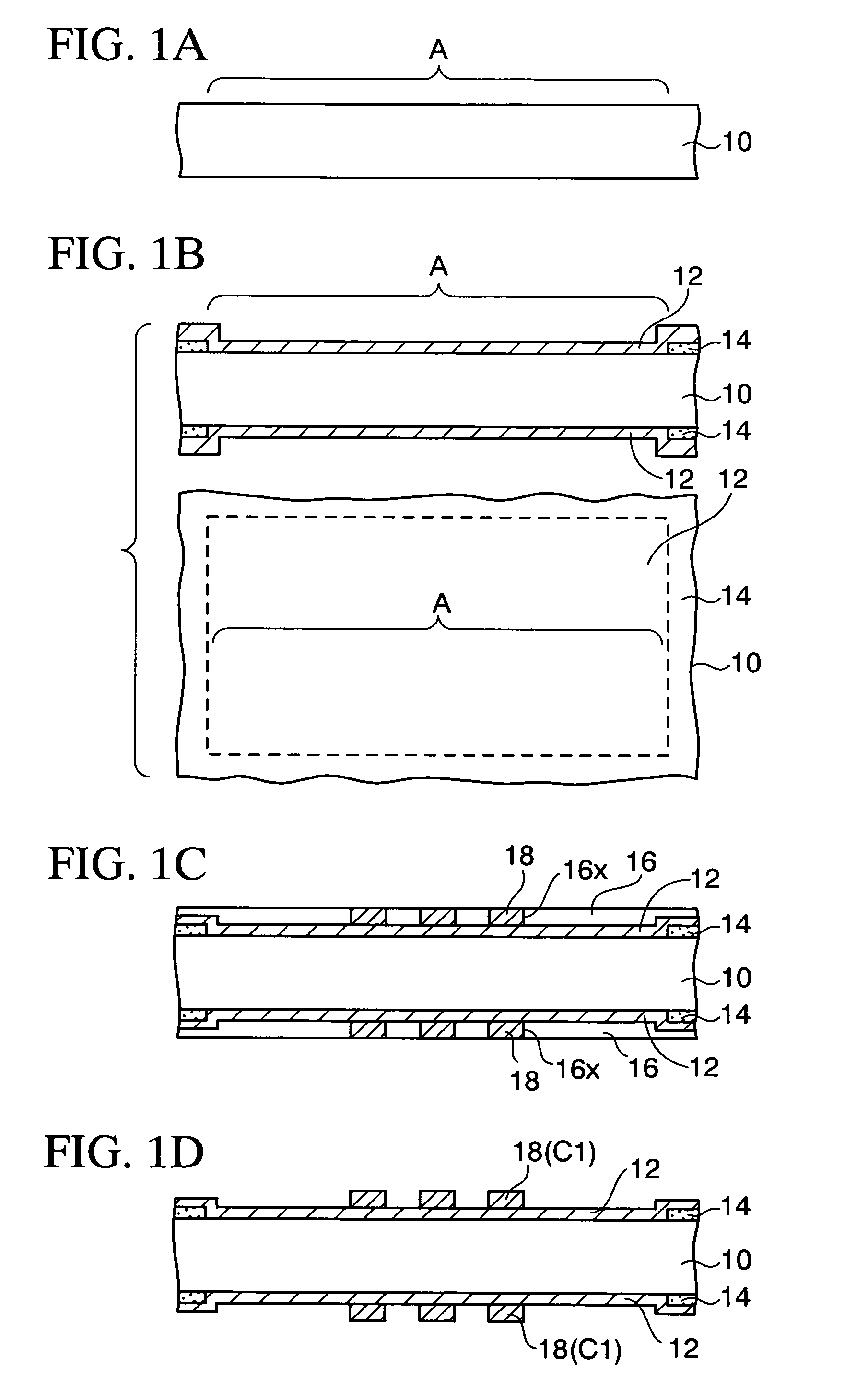
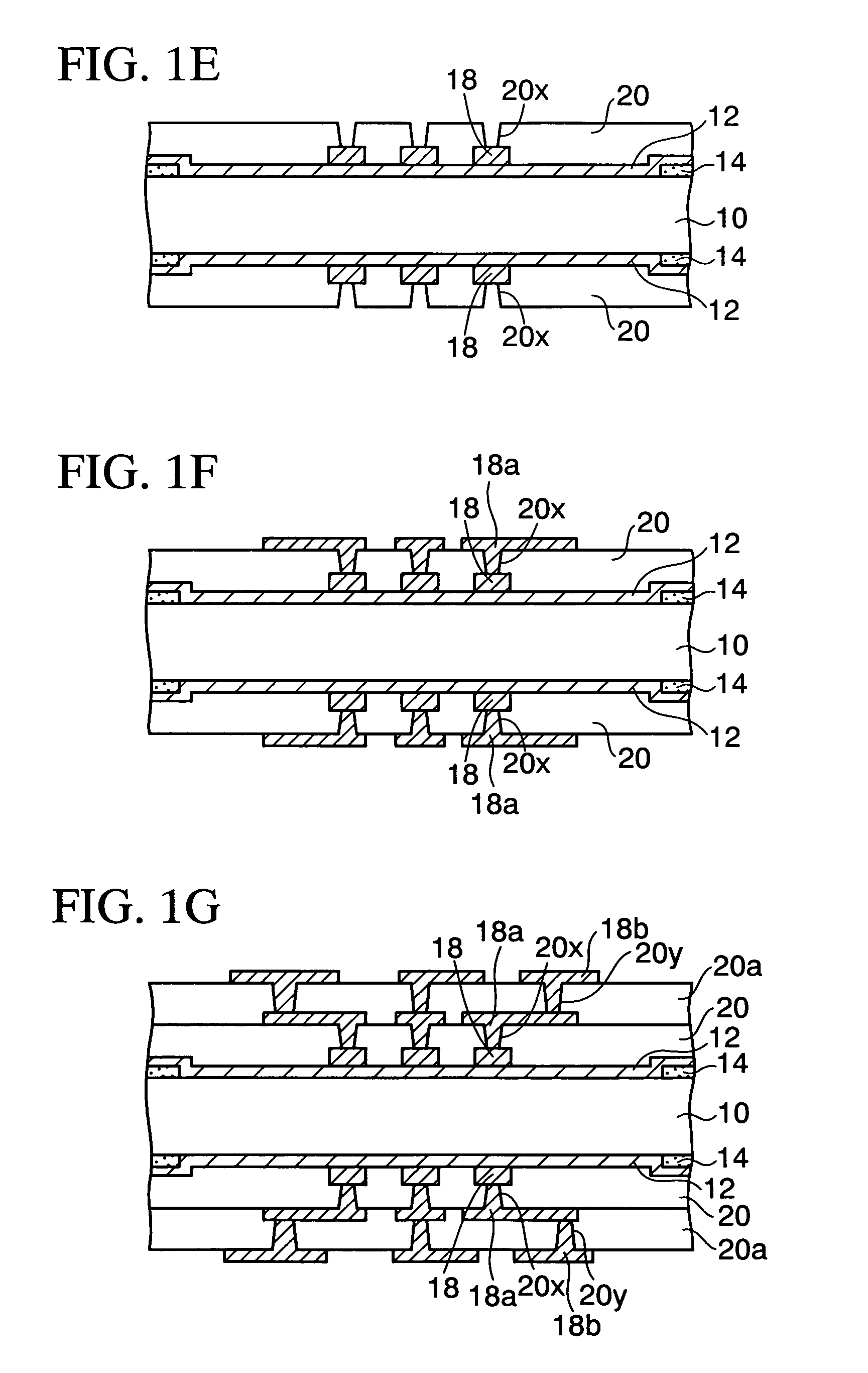
[0025]FIGS. 1A to 1K are cross-sectional views sequentially showing a method of manufacturing a wiring substrate according to a first embodiment of the present invention. First, as shown in FIG. 1A, a temporary substrate 10 made of a nonwoven glass fabric epoxy resin which is composed by impregnating a nonwoven glass fabric with epoxy resin is prepared. Otherwise, a temporary substrate 10 formed by impregnating a nonwoven fabric made of another fiber such as aramid or liquid crystal polymer and the like with resin can be used.

[0026] One of features of this embodiment is to approximate a thermal expansion coefficient of the temporary substrate 10 to a thermal expansion coefficient of a build-up wiring layer to be formed thereon. For this reason, the temporary substrate 10 made of the above-described materials is employed herein, and the thermal expansion efficient thereof is set in a range from 30 ppm / ° C. to 50 ppm / ° C. Meanwhile, wiring formation regions A for obtaining wiring sub...

second embodiment

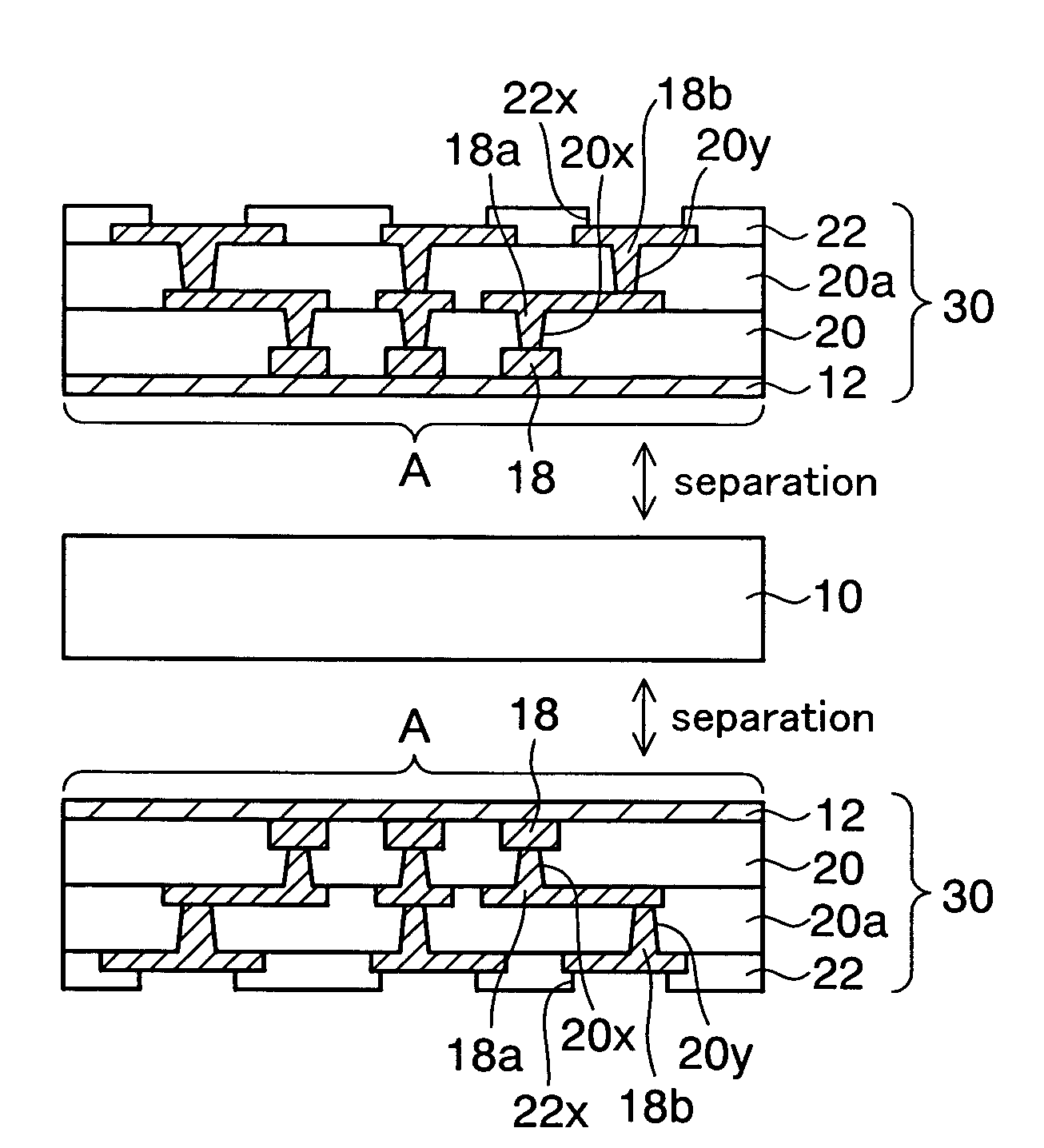
[0048]FIGS. 4A to 4F are cross-sectional views showing a method of manufacturing an electronic component mounting structure according to a second embodiment of the present invention. In the second embodiment, a preferred method of mounting an electronic component on a wiring substrate will be described based on a technical idea of the method of manufacturing a wiring substrate of the present invention.

[0049] First, as shown in FIG. 4A, a temporary substrate 10 made of a nonwoven glass fabric epoxy resin is prepared. Then, copper foils 12 are tentatively fixed to both surfaces of the temporary substrate 10, respectively, by selectively attaching peripheral sides of the copper foils 12 to outer peripheral portions of wiring formation regions A of the temporary substrate 10 with adhesive layers 14 as similar to the first embodiment.

[0050] Moreover, solder resist films 22a provided with openings 22y is formed on the copper foils 12 of the both surfaces side of the temporary substrate ...


PUM

PropertyMeasurementUnit
thicknessaaaaaaaaaa
temperatureaaaaaaaaaa
thermal expansion coefficientaaaaaaaaaa

Abstract

In a method of manufacturing a wiring substrate according to the present invention, a metal foil is tentatively fixed onto a temporary substrate, which is made of a nonwoven fabric impregnated with resin, by selectively attaching a peripheral side of the metal foil to an outer peripheral portion of a wiring formation region of the temporary substrate, thereafter, a build-up wiring layer is formed on the metal foil, and the metal foil is separated from the temporary substrate by cutting out an inside portion of a structure, the portion being inward from the adhesive layer, in this way, a wiring member including the build-up wiring layer formed on the metal foil is obtained.

Description

CROSS-REFERENCE TO RELATED APPLICATIONS [0001] This application is based on and claims priority of Japanese Patent Application No. 2005-353142 filed on Dec. 7, 2005, the entire contents of which are incorporated herein by reference. BACKGROUND OF THE INVENTION [0002] 1. Field of the Invention [0003] The present invention relates to a method of manufacturing a wiring substrate and a method of manufacturing an electronic component mounting structure. More specifically, the present invention relates to a method of manufacturing a wiring substrate applicable to a mount substrate for an electronic component, and to a method of manufacturing an electronic component mounting structure for mounting an electronic component on the wiring substrate. [0004] 2. Description of the Related Art [0005] As a wiring substrate for mounting an electronic component, there has heretofore been a method of obtaining a wiring substrate by forming a desired wiring layer on a temporary substrate in a detachabl...

Claims


Application Information

Patent Timeline
Patent Type & Authority Applications(United States)
IPC IPC(8): H05K1/11
CPCH01L21/6835Y10T29/49126H01L2224/16H01L2924/01078H01L2924/01079H01L2924/19041H05K3/205H05K3/4682H05K2201/0355H05K2203/0152H05K2203/0156H05K2203/0376H05K2203/0522H05K2203/0733H05K2203/1536Y10T29/49117Y10T29/49149Y10T29/49155Y10T29/4913Y10T29/49128H01L2221/68345H05K3/46H05K3/32
Inventor NAKAMURA, JUNICHI
Owner SHINKO ELECTRIC IND CO LTD
Why Eureka
Try Eureka