Eureka AIR delivers breakthrough ideas for toughest innovation challenges, trusted by R&D personnel around the world.

Ring-shaped electrode and manufacturing method for same

a technology of ring-shaped electrodes and manufacturing methods, which is applied in the direction of digital storage, instruments, semiconductor devices, etc., can solve the problems of increased resistance, lack of uniformity or reliability of large-scale memory devices, and limited cell manufacturing processes of standard integrated circuit manufacturing processes, etc., and achieves low resistance and high yield.

Active Publication Date: 2010-10-21
MACRONIX INT CO LTD +1
View PDF99 Cites 29 Cited by
  • Summary
  • Abstract
  • Description
  • Claims
  • Application Information

AI Technical Summary

Benefits of technology

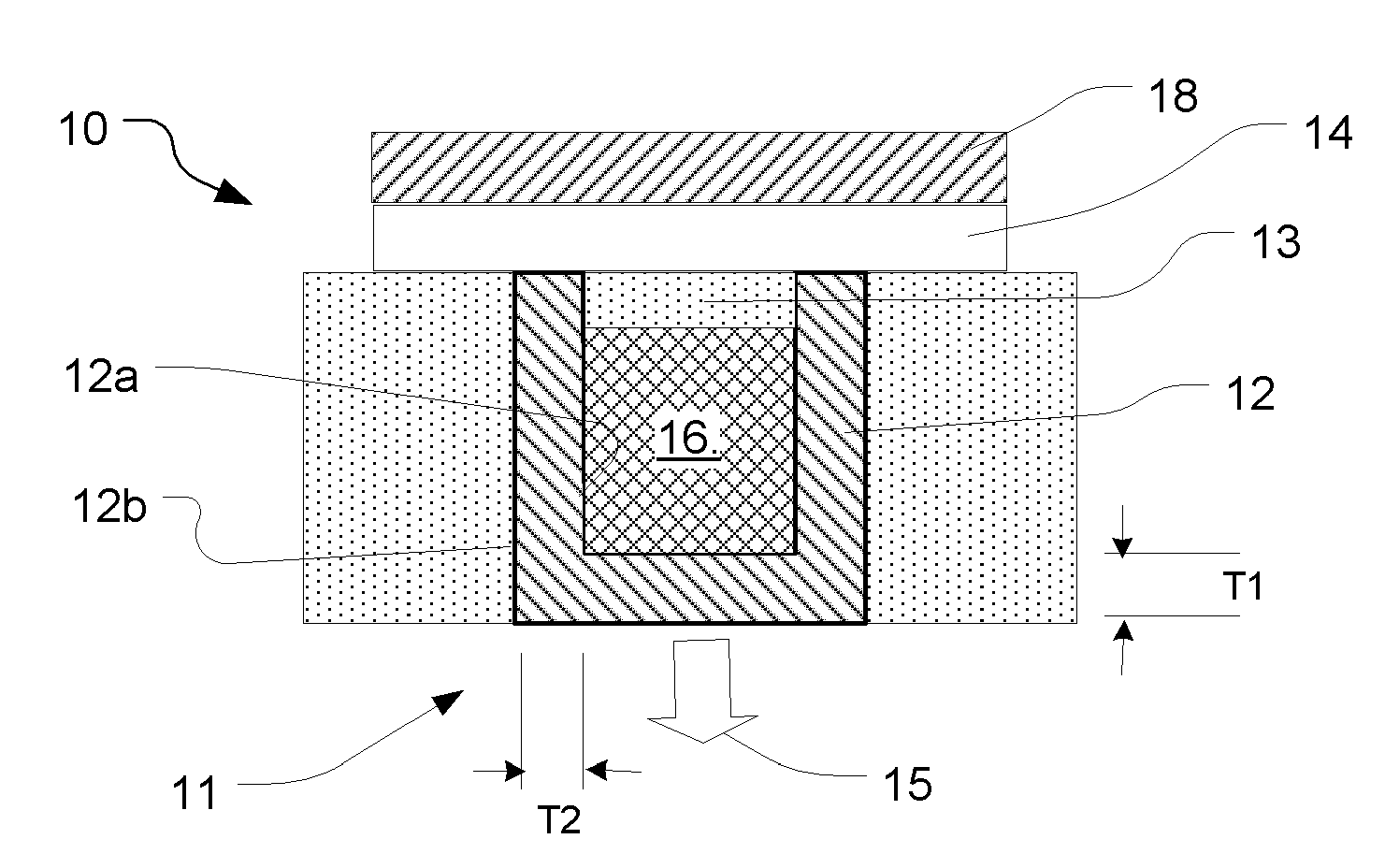
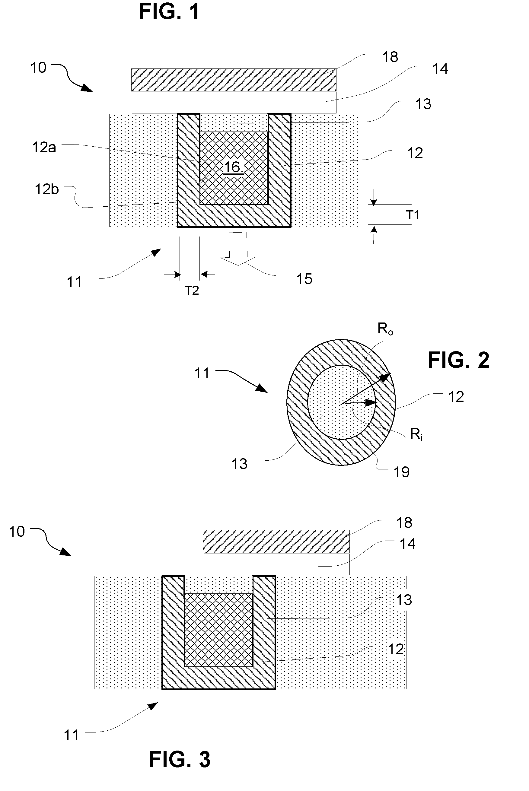
[0012]The present invention includes devices and methods to form an electrode structure for an integrated circuit device such as a memory cell, including a small, ring-shaped contact area, while maintaining low resistance and high yield.
[0013]An integrated circuit device is described comprising a pipe-shaped member of electrode material with a ring-shaped top surface. The pipe-shaped member has an axis, a first end and a second end. Side walls of electrode material form the pipe-shaped member with a thickness in a dimension orthogonal to the axis of the pipe-shaped member. A first end of the pipe-shaped member contacts an underlying contact element. Preferably, the first end of the pipe-shaped member is closed with electrode material, which can be the same as or different from that used to form the sidewalls. A second end of the pipe-shaped member has a ring-shaped surface that acts as the contact surface for the electrode. A first layer of conducting fill material is inside the inside surface of the pipe-shaped member. The first layer of conducting fill material comprises a conductive material. A second layer of insulating fill material is on top of the first layer of fill material inside the inside surface of the pipe-shaped member. The second layer of insulating fill material can be relatively thin so that the length of the pipe-shaped member which extends above the first layer of conducting fill material is short. As a result of the combination of conducting fill material and insulating fill material, the resistance of the electrode structure is significantly reduced. Also, the reliability in manufacturing of the electrode structure is improved. The conducting fill material can be a doped polysilicon, other silicon material, or other material characterized by being readily oxidized to form an insulating oxide. The second layer of fill material can be an oxide of the conducting fill material used to form the first layer of fill material. Thus, in examples where the first layer of fill material comprises silicon, the second layer of fill material comprises silicon dioxide. The resulting structure has a pipe-shaped element that has relatively lower resistance because of the conductivity of the first layer of fill material, while providing an easily manufactured ring-shaped contact surface.

Problems solved by technology

One problem associated with phase change memory devices arises because the magnitude of the current required for reset operations depends on the volume of phase change material that must change phase.
Thus, cells made using standard integrated circuit manufacturing processes have been limited by the minimum feature size of manufacturing equipment.
Thus, techniques to provide sublithographic dimensions for the memory cells must be developed, which can lack uniformity or reliability needed for large scale, high density memory devices.
One problem with ring-shaped electrodes arises from the increased resistance due to the small cross-sectional area of the electrode orthogonal to the current flow direction.
The increase in resistance requires a higher voltage across the memory cell to achieve a given current and increases the power consumption of the device.
It is difficult to manufacture such sidewall structures that have uniform thicknesses along the length of the electrode, particularly as the thicknesses of the sidewall structures used for the ring-shaped electrode fall below about 30 nanometers.
Thus, thin spots can occur in the thin-film sidewalls which may result in unevenness in current flow around the ring, and even discontinuities in the structure that can affect manufacturing yield.

Method used


Image

  • Ring-shaped electrode and manufacturing method for same
  • Ring-shaped electrode and manufacturing method for same
  • Ring-shaped electrode and manufacturing method for same

Examples


Embodiment Construction

[0027]The following detailed description is made with reference to the figures. Preferred embodiments are described to illustrate the present invention, not to limit its scope, which is defined by the claims. Those of ordinary skill in the art will recognize a variety of equivalent variations on the description that follows.

[0028]FIG. 1 is a simplified cross-sectional view of a phase change memory cell 10 including a pipe-shaped electrode having a ring-shaped top surface. The cell includes a bottom electrode 11 in contact with a terminal (schematically arrow 15) of an access structure. The bottom electrode includes a pipe-shaped member 12 having a first end adjacent the terminal 15, and a second end opposite the first. The pipe-shaped member 12 comprises an electrode material, such as TiN or other electrode materials. In the illustrated embodiment, the pipe-shaped member 12 is filled with conductive material 16, such as n-doped polysilicon that can be oxidized or nitridized as expla...


PUM


Abstract

An electrode structure and a method for manufacturing an integrated circuit electrode includes forming a bottom electrode comprising a pipe-shaped member, filled with a conductive material such as n-doped silicon, and having a ring-shaped top surface. A disc-shaped insulating member is formed on the top of the pipe-shaped member by oxidizing the conductive fill. A layer of programmable resistance material, such as a phase change material, is deposited in contact with the top surface of the pipe-shaped member. A top electrode in contact with the layer of programmable resistance material.

Description

PARTIES TO A JOINT RESEARCH AGREEMENT[0001]International Business Machines Corporation, a New York corporation; and Macronix International Corporation, Ltd., a Taiwan corporation, are parties to a Joint Research Agreement.BACKGROUND OF THE INVENTION[0002]1. Field of the Invention[0003]The present invention relates to ring-shaped electrodes usable in high density memory devices based on programmable resistance material, like phase change based memory materials, and to methods for manufacturing such devices.[0004]2. Description of Related Art[0005]Chalcogenide materials are widely used in read-write optical disks. These materials have at least two solid phases, generally amorphous and generally crystalline. Laser pulses are used in read-write optical disks to switch between phases and to read the optical properties of the material after the phase change.[0006]Chalcogenide materials also can be caused to change phase by application of electrical current. This property has generated int...

Claims


Application Information

Patent Timeline
IPC IPC(8): H01L47/00H01L21/283
CPCG11C13/0004H01L27/2436H01L45/04H01L45/06H01L45/085H01L45/1233H01L45/1675H01L45/142H01L45/144H01L45/146H01L45/16H01L45/1625H01L45/1641H01L45/1273
Inventor LUNG, HSIANG-LANCHEN, SHIH-HUNGROSSNAGEL, STEPHEN M.
Owner MACRONIX INT CO LTD
Why Eureka
Eureka Blog
Learn More