Method of manufacturing a piezoelectric thin film resonator, manufacturing apparatus for a piezoelectric thin film resonator, piezoelectric thin film resonator, and electronic component

a manufacturing apparatus and piezoelectric technology, applied in the direction of piezoelectric/electrostrictive/magnetostrictive devices, piezoelectric/electrostriction/magnetostriction machines, electrical apparatus, etc., can solve the problems of difficult to completely remove unnecessary parts of the metal film, the time required to completely etch the metal film changes every time etching is carried out, and the electric characteristics of the piezoelectric thin film element cannot meet the desired characteristics

Active Publication Date: 2007-07-03
SNAPTRACK
View PDF15 Cites 27 Cited by
  • Summary
  • Abstract
  • Description
  • Claims
  • Application Information

AI Technical Summary

Benefits of technology

[0007]The present invention was conceived in view of the problem described above and it is a principal object of the present invention to provide a method of manufacturing and a manufacturing apparatus that can reliably manufacture a piezoelectric thin film resonator with desired electrical characteristics, a piezoelectric thin film resonator manufactured according to this method of manufacturing, and an electronic component constructed so as to include this piezoelectric thin film resonator.
[0010]According to the above method of manufacturing and manufacturing apparatus for a piezoelectric thin film resonator, before an upper electrode is formed, a protective layer is formed so as to cover at least a part of a piezoelectric film where the upper electrode is not formed, so that when the electrode material layer is etched, the piezoelectric film is protected from corrosion by the etching liquid, which makes it possible to avoid unnecessary etching of the piezoelectric film and to carry out a sufficient etching to completely remove parts of the electrode material layer that are not covered by the mask. Accordingly, since it is possible to avoid problems such as variations in the thickness of the piezoelectric film or parts of the electrode material layer and the like remaining on the piezoelectric film, it is possible to reliably and easily manufacture a piezoelectric thin film resonator with the desired electrical characteristics. In this case, by not forming the protective layer in parts where the upper electrode is formed and only forming the protective layer in non-formed parts, it is possible to manufacture a piezoelectric thin film resonator with a high coupling coefficient.
[0011]In this method of manufacturing a piezoelectric thin film resonator, the protective layer should preferably be formed with silicon oxide (SiO2). According to this preferred aspect, it is possible to reliably protect the piezoelectric film from corrosion by an etching liquid for etching aluminum, gold, or the like.
[0012]In this method of manufacturing a piezoelectric thin film resonator, the piezoelectric film should preferably be formed with zinc oxide (SiO). According to this preferred aspect, it is possible to manufacture a piezoelectric thin film resonator with a large passing bandwidth in the filter characteristics. In this case, according to this method of manufacturing, the piezoelectric film is reliably protected by the protective layer, so that even in the case where the piezoelectric film is formed using ZnO that is easily corroded by acid, such as acetic acid, phosphoric acid, and nitric acid, included in the etching liquid, a piezoelectric thin film resonator with the desired electrical characteristics can be easily and reliably manufactured.
[0013]Also, according to this method of manufacturing a piezoelectric thin film resonator, the electrode material layer should preferably be formed with aluminum (Al) or gold (Au). According to this preferred aspect, it is possible to manufacture a piezoelectric thin film resonator with a sufficiently high resonance frequency. In addition by forming the electrode material layer with gold, it is possible to manufacture a piezoelectric thin film resonator with a low insertion loss for passing signals.
[0014]Also, according to this method of manufacturing and manufacturing apparatus for a piezoelectric thin film resonator, the upper electrode should preferably be formed by etching the electrode material layer by wet etching. According to this preferred aspect, it is possible to easily and reliably manufacture a piezoelectric thin film resonator using relatively simple manufacturing equipment.

Problems solved by technology

In this case, if the piezoelectric film is etched or parts of the metal film unintentionally remain, the electrical characteristics of the piezoelectric thin film element will not satisfy the desired characteristics for which the piezoelectric thin film element was designed.
However, the time required to completely etch the metal film changes every time etching is carried out due to factors such as minute variations in the thickness of the metal film and changes in the temperature of the etching liquid.
Accordingly, with the conventional method of manufacturing a piezoelectric thin film element, there is the problem that it is difficult to completely remove unnecessary parts of the metal film without etching the piezoelectric film when forming the upper electrode.

Method used


Image

  • Method of manufacturing a piezoelectric thin film resonator, manufacturing apparatus for a piezoelectric thin film resonator, piezoelectric thin film resonator, and electronic component
  • Method of manufacturing a piezoelectric thin film resonator, manufacturing apparatus for a piezoelectric thin film resonator, piezoelectric thin film resonator, and electronic component
  • Method of manufacturing a piezoelectric thin film resonator, manufacturing apparatus for a piezoelectric thin film resonator, piezoelectric thin film resonator, and electronic component

Examples


Embodiment Construction

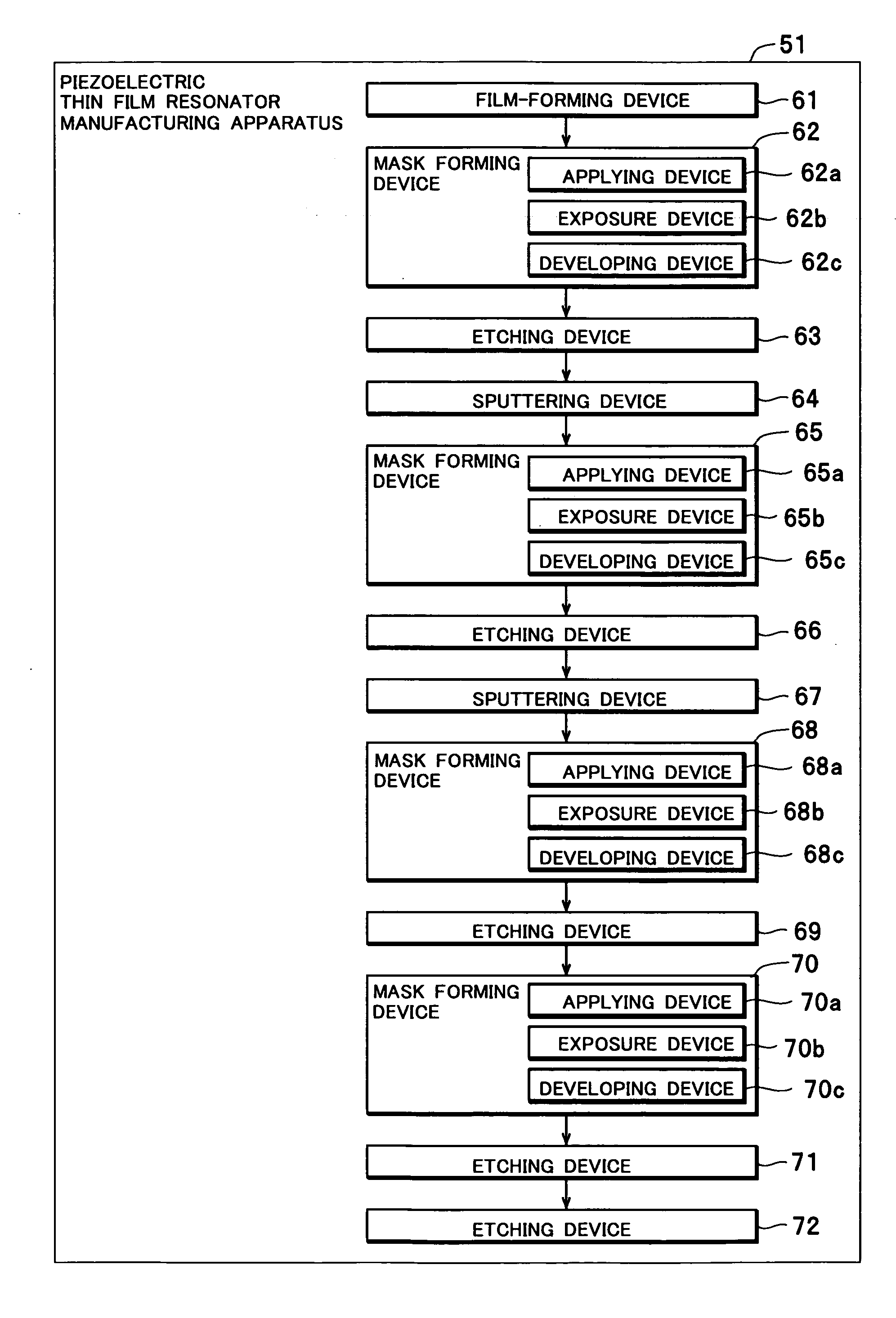
[0045]Hereafter, preferred embodiments of a method of manufacturing and a manufacturing apparatus for a piezoelectric thin film resonator according to the present invention, a piezoelectric thin film resonator manufactured according to this method of manufacturing, and an electronic component constructed so as to include this piezoelectric thin film resonator will be described with reference to the attached drawings.

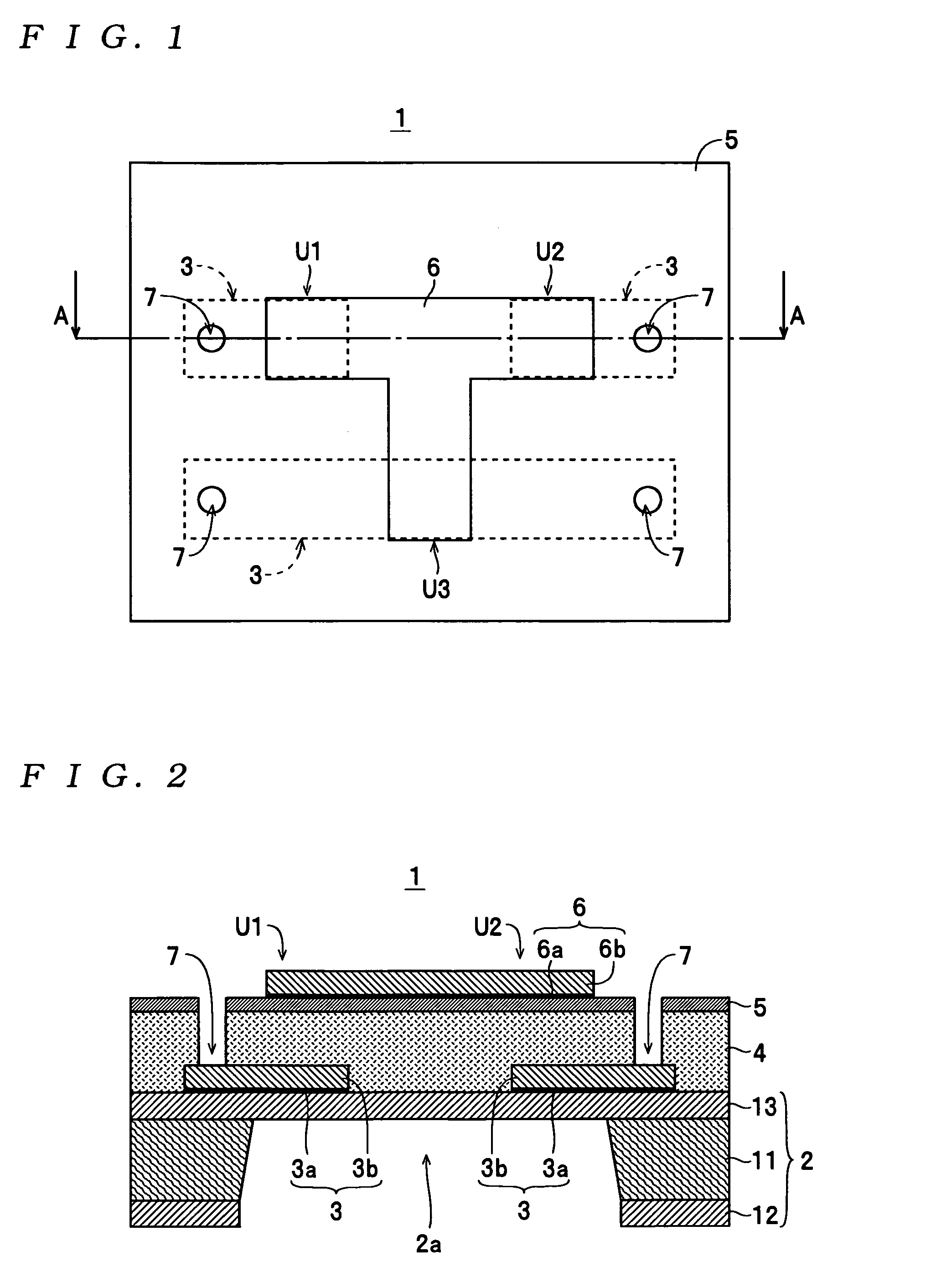
[0046]First, the construction of a piezoelectric thin film resonator 1 will be described with reference to the drawings.

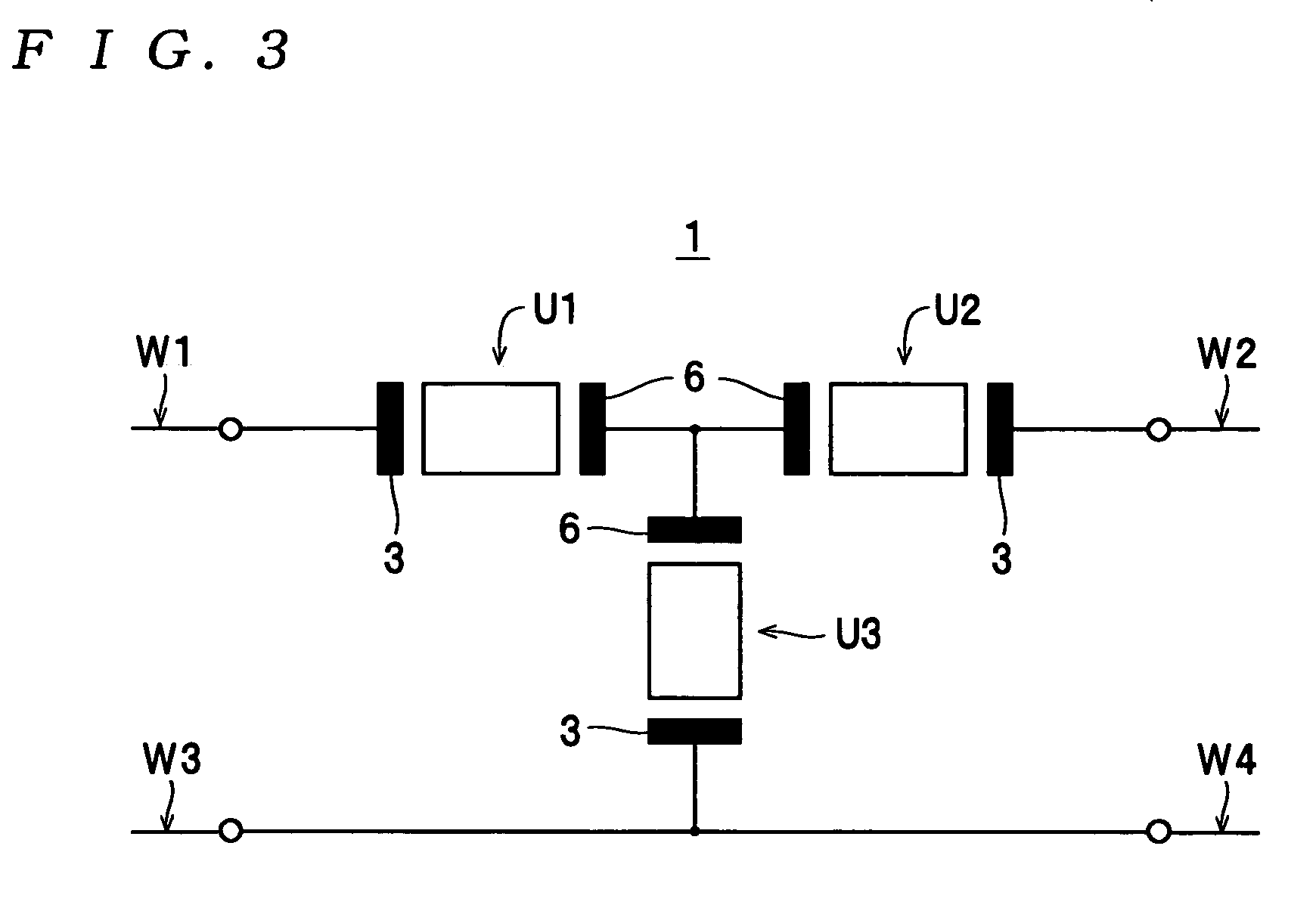
[0047]The piezoelectric thin film resonator 1 shown in FIGS. 1 and 2 corresponds to the piezoelectric thin film resonator according to the present invention, and is constructed so as to include a substrate 2, lower electrodes 3, 3, 3, a piezoelectric film 4, a protective layer 5 and an upper electrode 6. In this case, the piezoelectric thin film resonator 1 is constructed so as to include three unit piezoelectric thin film resonators U1 to U3 (hereinaft...


PUM

PropertyMeasurementUnit
thicknessaaaaaaaaaa
thicknessaaaaaaaaaa
thicknessaaaaaaaaaa

Abstract

A method of manufacturing a piezoelectric thin film resonator forms, after forming a piezoelectric film on a substrate so as to cover a lower electrode formed on the substrate, an electrode material layer for forming an upper electrode above the piezoelectric film, forms a mask of a predetermined form on the electrode material layer, and then etches the electrode material layer to form the upper electrode. Before a step of forming the electrode material layer, a protective layer for protecting the piezoelectric film during etching of the electrode material layer is formed so as to cover at least a part of the piezoelectric film where the upper electrode is not formed, and the electrode material layer is then formed so as to cover the protective layer.

Description

BACKGROUND OF THE INVENTION[0001]1. Field of the Invention[0002]This invention relates to a method of manufacturing and a manufacturing apparatus for a piezoelectric thin film resonator in which a lower electrode, a piezoelectric film, and an upper electrode are formed in order on a substrate, a piezoelectric thin film resonator manufactured according to this method of manufacturing, and an electronic component constructed so as to include this piezoelectric thin film resonator.[0003]2. Description of the Related Art[0004]As one example of a piezoelectric thin film resonator manufactured according to this kind of method of manufacturing, a piezoelectric thin film element for use as a filter or the like in an electronic appliance, such as a mobile phone, is disclosed by Japanese Laid-Open Patent Publication No. 2001-251159. This piezoelectric thin film element is constructed by forming a lower electrode, a piezoelectric film, and an upper electrode in that order on a silicon substrat...

Claims


Application Information

Patent Timeline
Patent Type & Authority Patents(United States)
IPC IPC(8): H01L41/00H01B13/00H02N2/00H03H9/17H03H3/02H03H9/56
CPCH03H3/02H03H9/564
Inventor KOMURO, EIJUSAITOU, HISATOSHINOGUCHI, TAKAOIMURA, MASAAKI
Owner SNAPTRACK
Why Eureka
Try Eureka