

Coating strip of cavity surface of semiconductor laser and preparation method thereof
A technology of lasers and semiconductors, applied in semiconductor lasers, structural details of semiconductor lasers, lasers, etc., can solve problems that affect laser loss, life and stability, and are prone to "shadows" to improve stability and service life. The effect of the "shadow" effect
- Summary
- Abstract
- Description
- Claims
- Application Information
AI Technical Summary
Problems solved by technology
Method used
Image

Examples
Embodiment 1
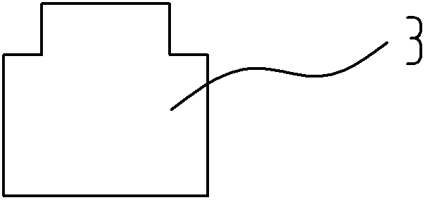
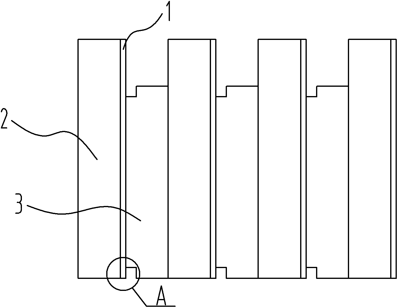
[0023] Embodiment one: see Figure 1~Figure 4 As shown, a semiconductor laser cavity surface coating strip is used to separate the two laser bars when the laser bar 2 is coated. The coating strip 3 is a strip with a convex cross section, and the coating strip 3 The width is shorter than the width of the laser bar 2.
[0024] In the first embodiment, the semiconductor laser is a GaN-based semiconductor laser, the cavity length of the coated cavity surface is 600um, and the length of the semiconductor laser bar is 9.6mm.
[0025] The preparation method of the coating spar on the cavity surface of the semiconductor laser comprises the following steps:
[0026] (1) Select Si sheet as the substrate for preparing the coating spatula;
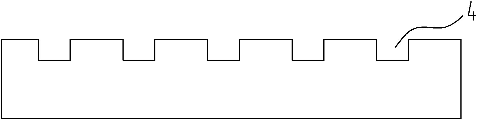
[0027] (2) Process five grooves 4 with a depth of 40 um and a width of 150 um at intervals of 550 um on one surface of the substrate in step (1);
[0028] (3) Cleavage the substrate obtained in step (2) along the axial direction of each groove 4 in...
PUM
| Property | Measurement | Unit |
|---|---|---|
| Depth | aaaaa | aaaaa |
| Width | aaaaa | aaaaa |
Abstract
Description
Claims
Application Information