

Flash memory chip analysis method and device, electronic equipment and storage medium
A flash memory chip and analysis method technology, applied in the computer field, can solve the problems of unstable use and low service life of flash memory chips, and achieve the effect of improving service life and stability
- Summary
- Abstract
- Description
- Claims
- Application Information
AI Technical Summary
Problems solved by technology
Method used
Image

Examples
Embodiment 1
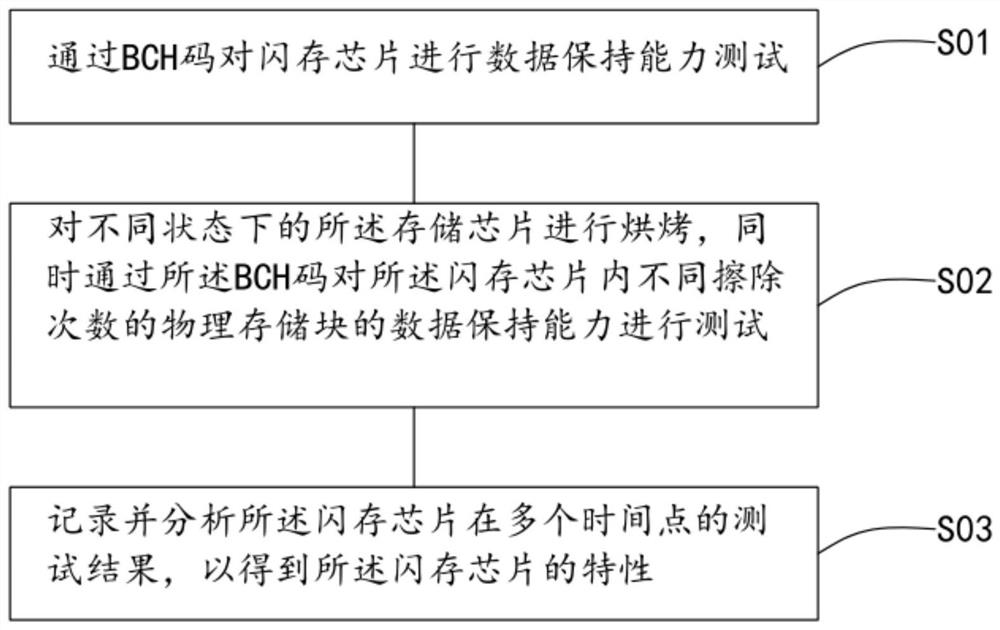
[0042] For a flash memory chip analysis method provided in the first embodiment of the present invention, please refer to figure 1 , the method includes step S01 to step S03:
[0043] Step S01 , performing a data retention capability test on the flash memory chip through the BCH code.
[0044] Step S02 , baking the memory chips in different states, and at the same time testing the data retention capabilities of the physical memory blocks in the flash memory chip with different erasing times through the BCH code.
[0045] Step S03, recording and analyzing the test results of the flash memory chip at multiple time points to obtain the characteristics of the flash memory chip.
[0046] Specifically, in this embodiment, the data retention capability (i.e. data retention) test of the flash chip with low erasing times is tested, wherein the flashing chip with low erasing times is a flash memory chip that has just been produced and processed, and the number of times of use is small,...
Embodiment 2
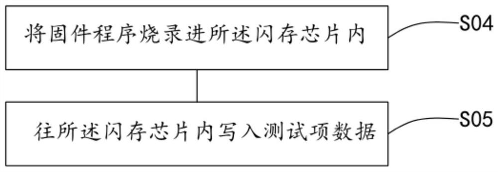
[0050] For an embodiment of the invention, see figure 2 , before step S02, the method also includes step S04 to step S05:
[0051] Step S04, burning the firmware program into the flash memory chip.
[0052] Step S05, writing test item data into the flash memory chip.
[0053] Specifically, use the characteristic analysis software to burn the firmware program to the flash memory chip and perform the erase, write and read test of the private command, so that the number of erases of the specified physical memory block reaches the required value, read the original ECC data and put it into a constant temperature and humidity box. Rest Bake simulates actual data placement for one, two, or many years in actual use.
Embodiment 3
[0055] In another embodiment of the present invention, after the step of burning the firmware program into the flash memory chip, the method further includes the following steps:
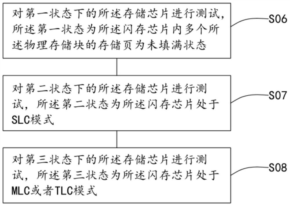
[0056] Step S06 , testing the memory chip in a first state, the first state being that the memory pages of the plurality of physical memory blocks in the flash memory chip are not full.
[0057] Specifically, when each storage page of the physical storage block is filled with data, the physical storage block is in a closed state; when there are some blank storage pages in the physical storage block, the physical storage block is in an open state;
[0058] Through the above method, when using the simulation platform, if the written data exceeds the storage capacity of one or more physical storage blocks, after firmware processing, part of the physical lookup of the flash memory will be closed, and some physical storage blocks will be closed due to If the data is not full, it is in an open state to si...
PUM
 Abstract
Description
Claims
Application Information