Circuit board with double-sided universal circuit layout and layout method thereof

A technology of circuit layout and general circuit, applied in the direction of printed circuit, printed circuit manufacturing, printed circuit components, etc., can solve the problems of increasing manufacturing cost and inventory pressure, and the inability to share circuit boards.

Inactive Publication Date: 2012-07-04
ASKEY COMP
View PDF3 Cites 2 Cited by
  • Summary
  • Abstract
  • Description
  • Claims
  • Application Information

AI Technical Summary

Problems solved by technology

Therefore, only the lower integrated circuit components 1 and inductors 8 can be arranged on the surface of the circuit board 2 in contact with the casing.
The higher resistor 4 and capacitor 6 cannot be set on this side, but must be set on the other side of the circuit board
[0007] As mentioned above, the existing technology makes different designs for the circuit boards of the indoor equipment and the outdoor equipment, which cannot be shared, thereby increasing the manufacturing cost and inventory pressure

Method used


Image

  • Circuit board with double-sided universal circuit layout and layout method thereof
  • Circuit board with double-sided universal circuit layout and layout method thereof
  • Circuit board with double-sided universal circuit layout and layout method thereof

Examples


Embodiment Construction

[0029] In order to fully understand the purpose, features and effects of the present invention, the present invention will be described in detail by means of the following specific embodiments and accompanying drawings, as follows:

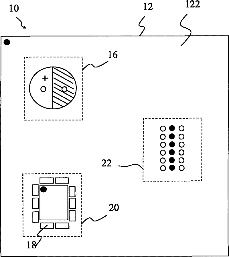
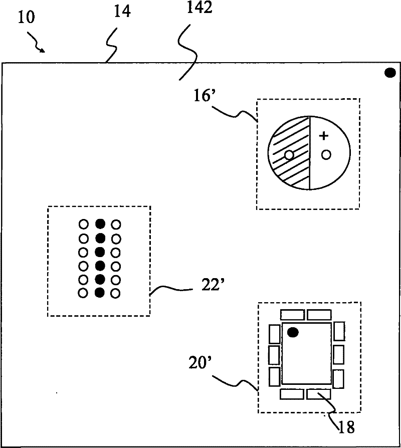
[0030] refer to Figure 2A and Figure 2B , are the circuit layout diagrams of the first side and the second side of the circuit board with double-sided universal circuit layout, respectively, according to an embodiment of the present invention. Wherein, the circuit board 10 with a double-sided universal circuit layout is used to provide electronic component placement, and the circuit board 10 has a first surface 12 and a second surface 14 opposite to each other.

[0031] At Figure 2A Among them, a first circuit layout 122 is provided on the first surface 12 of the circuit board 10. For example, the first circuit layout 122 can correspond to a plurality of electrical connection points of electronic components and the electrical properties betwe...


PUM


Abstract

A circuit board with double-sided universal circuit layout for laying out electronic components has a first side with a first circuit layout thereon and an opposing second side with a second circuit layout thereon; hence, the first circuit layout and the second circuit layout are disposed on the opposing sides of the circuit board, respectively. The first circuit layout and the second circuit layout feature electronic circuits having the same function, thereby allowing users to selectively install the electronic components at one of the first circuit layout and the second circuit layout as needed and still have access to the electronic circuits having the same function. A layout method for use with the circuit board with double-sided universal circuit layout is further introduced.

Description

technical field [0001] The invention relates to a circuit board with double-sided universal circuit layout and its layout method, in particular to a circuit board and its layout method for electronic components to be placed on both sides of the circuit board arbitrarily. Background technique [0002] With the rapid development of broadband networks and digital information, a large number of information and communication network equipment are widely distributed in various places to provide such as wireless network access devices (Access Point, AP), personal digital assistants (Personal Digital Assistant, PDA), The use of communication products such as notebook computers and portable mobile devices enables the above-mentioned devices to provide more convenient, more efficient and more service functions. [0003] In addition, the above-mentioned information communication network equipment can be further divided into outdoor equipment and indoor equipment according to the settin...

Claims


Application Information

Patent Timeline
Patent Type & Authority Applications(China)
IPC IPC(8): H05K1/02
CPCH05K2203/1572H05K1/111H05K1/0295
Inventor 彭国展谢青峰
Owner ASKEY COMP
Why Eureka
Try Eureka