
Bus bar, printed circuit board (PCB) and surface mounting method of bus bar

A PCB circuit board and PCB board technology, which is applied in the direction of assembling printed circuits with electrical components, printed circuits connected with non-printed electrical components, root rods/rods/wires/strip conductors, etc., can solve the problem of unsatisfactory effects and increased Problems such as tooling cost and affecting the heat conduction effect of bus bars can prevent poor contact from affecting heat conduction and improve life and reliability.

Inactive Publication Date: 2012-07-04
SHENZHEN MEGMEET ELECTRICAL CO LTD
View PDF7 Cites 3 Cited by
  • Summary
  • Abstract
  • Description
  • Claims
  • Application Information

AI Technical Summary

Problems solved by technology

[0003] In the manufacturing process of PCB circuit boards with bus bars, the traditional process adopts solder paste process and soldering with reflow soldering, but for slender bus bars with large area, due to the deformation of the bus bars themselves, improper manual Due to chain vibration and other reasons, the bus bar may be displaced during the SMT process, thus affecting the heat conduction effect of the bus bar
In the SMT process, although some auxiliary positioning fixtures can be used to solve this problem, the effect is not ideal, and the tooling cost will also be increased

Method used


Image

  • Bus bar, printed circuit board (PCB) and surface mounting method of bus bar
  • Bus bar, printed circuit board (PCB) and surface mounting method of bus bar
  • Bus bar, printed circuit board (PCB) and surface mounting method of bus bar

Examples


Embodiment Construction

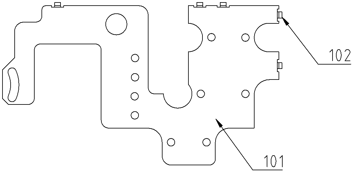
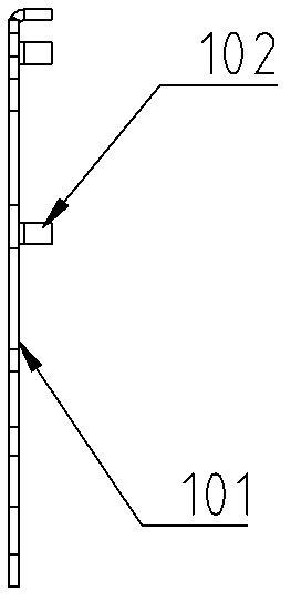
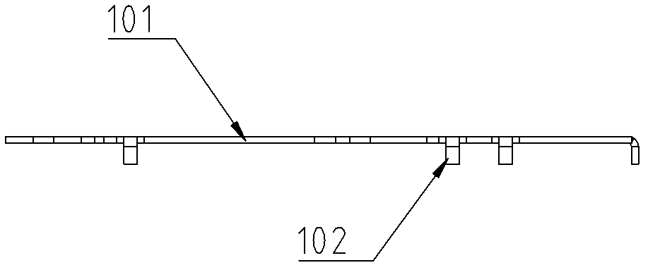
[0035] The structure of the bus bar in Embodiment 1 of the present invention is as follows Figure 1 to Figure 4 As shown, it includes a board body 101 and five positioning feet 102 . The five positioning feet 102 are located on the edge of the board body 101 , formed by extending and bending the edge of the board body 101 , and the five positioning feet 102 are perpendicular to the board body 101 .

[0036] The structure of the bus bar in embodiment 2 of the present invention is as follows Figure 5 to Figure 7 As shown, the three positioning pins 102 are positioning pins, and the plate body 101 is provided with the same number of pin holes as the positioning pins 102, and the positioning pins 102 are fixed in the pin holes through interference, and the three positioning pins 102 are perpendicular to the plate body 101.

[0037] The structure of the PCB circuit board of embodiment 3 of the present invention is as Figure 5 to Figure 7 As shown, including the bus bar 1 in th...


PUM


Abstract

The invention discloses a bus bar, a printed circuit board (PCB) and a surface mounting method of the bus bar. The bus bar is inserted into a locating hole of the PCB to be located through a locating pin of the bus bar or inserted into locating holes of the bus bar and the PCB to be located through an auxiliary locating pin to be soldered by adopting reflow soldering or wave soldering. The bus bar has a self-locating function, solves the problem that a slender bus bar with large area is easy to shift during a surface mount technology (SMT) manufacturing process, can prevent heat conduction from being affected caused by poor contact between the bus bar and the PCB, prolongs service life of products, and improves reliability of the products.

Description

[technical field] [0001] The invention relates to a printed circuit board, in particular to a bus bar, a PCB circuit board and a mounting method for the bus bar. [Background technique] [0002] The bus bar is attached to the PCB board, which plays the role of carrying large current and conducting heat. It is often used on circuit boards of high-power products. [0003] In the manufacturing process of PCB circuit boards with bus bars, the traditional process adopts solder paste process and soldering with reflow soldering, but for slender bus bars with large area, due to the deformation of the bus bars themselves, improper manual Due to chain vibration and other reasons, the bus bar may be displaced during the SMT process, thereby affecting the heat conduction effect of the bus bar. In the SMT process, although some auxiliary positioning fixtures can be used to solve this problem, the effect is not ideal, and the tooling cost will also be increased. [Content of the inventi...

Claims


Application Information

Patent Timeline
Patent Type & Authority Applications(China)
IPC IPC(8): H05K3/34H05K1/18H01B5/02
Inventor 赵英军吴坤李湘斌胡天鹏
Owner SHENZHEN MEGMEET ELECTRICAL CO LTD
Learn More