
Light emitting diode package and method for manufacturing same

A technology of light-emitting diodes and packaging structures, which is applied in the direction of electrical components, electric solid-state devices, circuits, etc., can solve the problems of unreduced manufacturing costs, cumbersome manufacturing processes, and complex structures, so as to save manufacturing costs, increase luminous flux, and simplify packaging. The effect of steps

Active Publication Date: 2012-07-11
EPISTAR CORP
View PDF10 Cites 6 Cited by
  • Summary
  • Abstract
  • Description
  • Claims
  • Application Information

AI Technical Summary

Problems solved by technology

Not only the structure is relatively complicated, but also more than two molding steps must be used, and the manufacturing process is relatively cumbersome, so that the manufacturing cost cannot be reduced

Method used


Image

  • Light emitting diode package and method for manufacturing same
  • Light emitting diode package and method for manufacturing same
  • Light emitting diode package and method for manufacturing same

Examples


Embodiment Construction

[0033] In order to further explain the technical means and effects of the present invention to achieve the intended purpose of the invention, the specific implementation methods, methods, Steps, structure, features and effects are described in detail below.

[0034] The aforementioned and other technical contents, features and effects of the present invention will be clearly presented in the following detailed description of the preferred embodiments with reference to the drawings. Through the description of the specific implementation, one can have a deeper and more specific understanding of the technical means and effects of the present invention to achieve the intended purpose. However, the attached drawings are only for reference and description, and are not used to limit the present invention. .

[0035] The object of the present invention is to provide a light emitting diode packaging structure and a manufacturing method thereof. Please refer to Figure 4A to Figure 4...


PUM


Abstract

A light emitting diode (LED) package and the manufacturing method thereof are provided. The LED package (400) comprises a substrate (404), at least one LED die (403), a lens (410) and an in-mold decoration film (40), wherein the LED die (403) is fixed on the substrate (404); the lens (410) is convexly molded on the substrate (404) to encapsulate the LED die (403); and the in-mold decoration film (40) has at least one phosphor layer (401) disposed on the lens (410) and a surface treatment layer (406) disposed on the phosphor layer (401).

Description

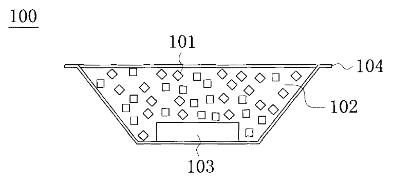
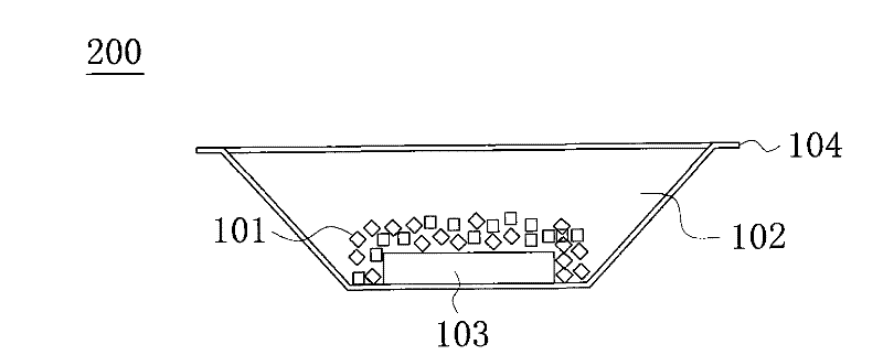
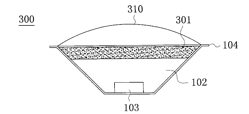
technical field [0001] The invention relates to a light emitting diode (Light Emitting Diode; LED) packaging structure and a manufacturing method thereof. Background technique [0002] With the increasing emphasis on energy saving and power saving, LED lighting has become one of the most concerned application fields. Please refer to Figure 1 to Figure 3 , Figure 1 to Figure 3 It is a partial structural schematic diagram of three light-emitting diode packaging structures according to the prior art. in figure 1 The packaging method of the light emitting diode packaging structure 100 is to use the most traditional uniform distribution technology to uniformly disperse the phosphor powder 101 in the encapsulant 102 on the surface of the substrate 104 . [0003] Because of this phosphor powder coating method, the dispersion uniformity of the phosphor powder 101 cannot be controlled, and the requirements of high color uniformity and high output lumen cannot be met. The indust...

Claims


Application Information

Patent Timeline
Patent Type & Authority Applications(China)
IPC IPC(8): H01L33/52H01L33/58
CPCH01L33/507H01L33/54H01L25/0753H01L33/44H01L2933/005H01L2933/0041H01L2933/0025H01L33/505H01L2924/0002H01L2924/00H01L33/50H01L33/52H01L33/58H01L33/56
Inventor 刘弘智
Owner EPISTAR CORP
Learn More