Multi-layer circuit board and electrostatic discharge protection structure
一种静电放电保护、多层电路板的技术,应用在电路静电放电保护、过电压保护、静电等方向,能够解决电路板设计尺寸越来越小、增加制造成本、增加电路复杂度等问题,达到良好静电防护效果的效果
- Summary
- Abstract
- Description
- Claims
- Application Information
AI Technical Summary
Problems solved by technology
Method used
Image

Examples
Embodiment Construction
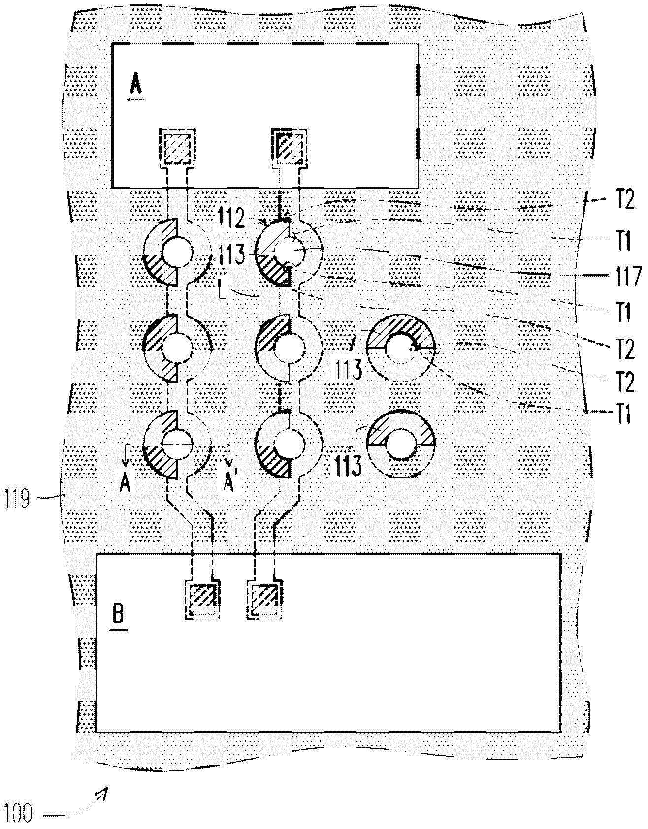
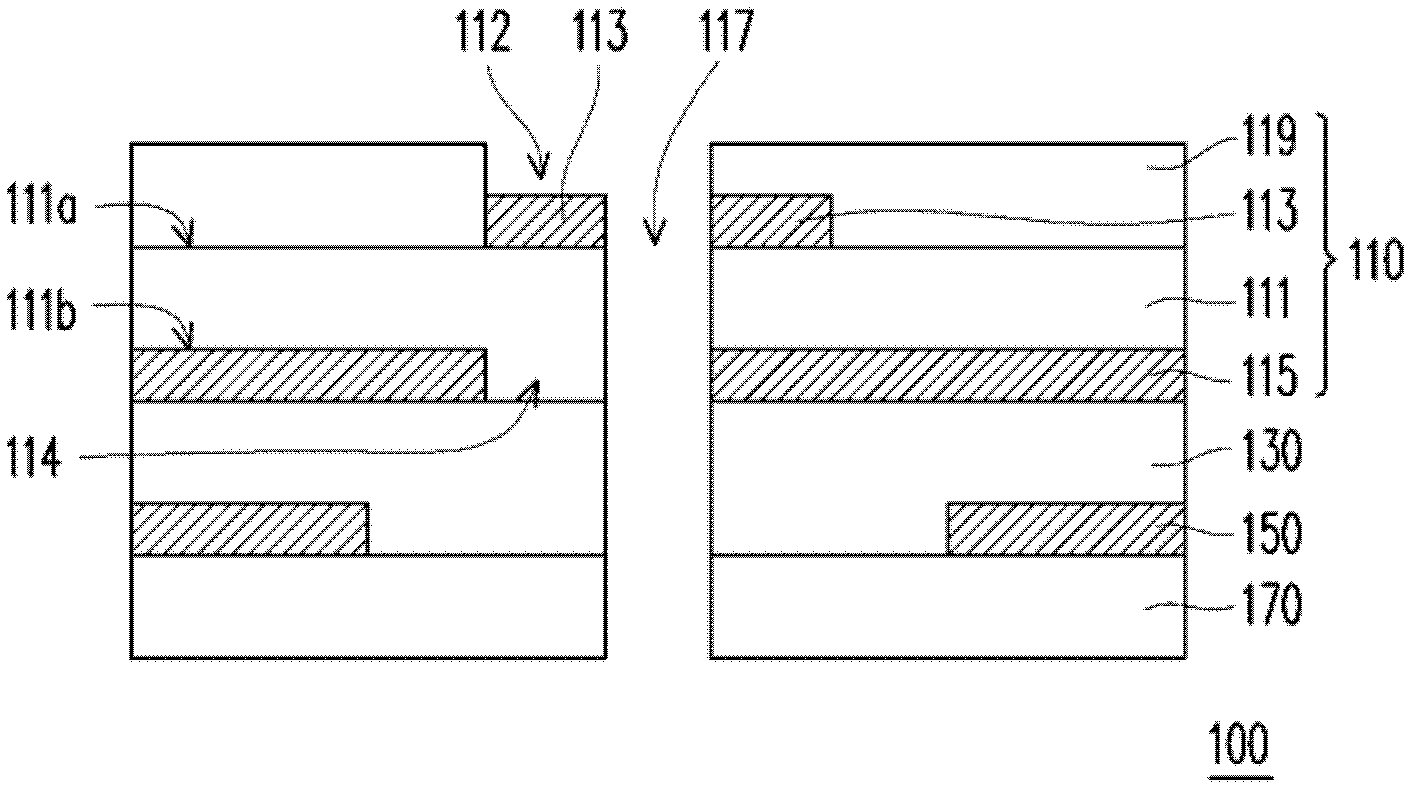
[0047] figure 1 It is a schematic top view of a multilayer circuit board according to an embodiment of the present invention, and Figure 2A for along figure 1 The cross-sectional schematic diagram of the A-A' section in . Please also refer to figure 1 and Figure 2A, the multilayer circuit board 100 of this embodiment is integrated with an electrostatic discharge protection structure 110 . In detail, the ESD protection structure 110 is integrated with the traces in the multilayer circuit board 100 to enhance the reliability of the multilayer circuit board 100 .
[0048] In this embodiment, the ESD protection structure 110 includes a first insulating layer 111 , a patterned conductive layer 113 and an ESD release layer 115 . When the ESD protection structure 110 is integrated into the multilayer circuit board 100 , the core layer, the laminated dielectric layer or the build-up dielectric layer in the multilayer circuit board 100 up dielectric layer) can be used as the fi...
PUM
 Abstract
Description
Claims
Application Information
 - Generate Ideas
- Intellectual Property
- Life Sciences
- Materials
- Tech Scout
- Unparalleled Data Quality
- Higher Quality Content
- 60% Fewer Hallucinations
Browse by: Latest US Patents, China's latest patents, Technical Efficacy Thesaurus, Application Domain, Technology Topic, Popular Technical Reports.
© 2025 PatSnap. All rights reserved.Legal|Privacy policy|Modern Slavery Act Transparency Statement|Sitemap|About US| Contact US: help@patsnap.com