Electrostatic protection device structure

A device structure, electrostatic protection technology, applied in the direction of electric solid devices, electrical components, semiconductor devices, etc., can solve problems such as weak self-protection ability, and achieve the effect of reducing area and area

Inactive Publication Date: 2015-02-04
SHANGHAI HUAHONG GRACE SEMICON MFG CORP
View PDF3 Cites 8 Cited by
  • Summary
  • Abstract
  • Description
  • Claims
  • Application Information

AI Technical Summary

Problems solved by technology

[0003] For products used in power management, the electrostatic protection solution adopts a self-protection solution due to its large area, such as figure 1 , that is, the protected circuit itself has a certain electrostatic discharge capability, and no additional electrostatic protection measures are required; structure as a power device, although the ESD protection capability is sufficient, its area may be more than double that of ordinary devices, mainly because the distance L from the metal contact hole in the drain region or source region to the polysilicon gate is compared with ordinary devices It is much larger, and the size of L is directly related to the electrostatic protection ability of this device. The larger L is, the stronger the electrostatic protection ability is.

Method used


Image

  • Electrostatic protection device structure
  • Electrostatic protection device structure
  • Electrostatic protection device structure

Examples


Embodiment Construction

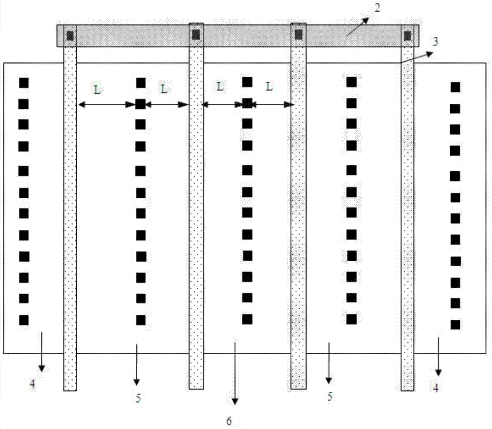
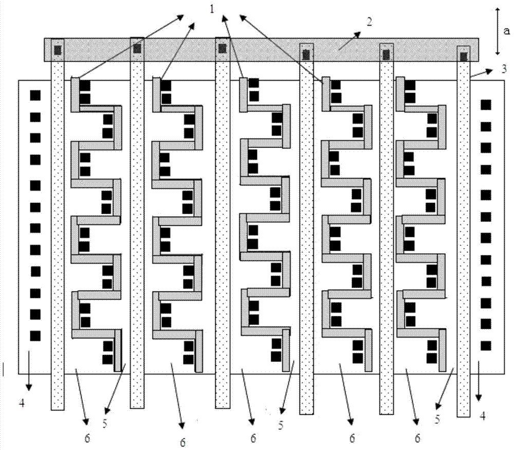
[0024] Such as figure 2 , image 3 As shown, the structure of the electrostatic protection device of the present invention, taking the N-type MOS transistor as an example, defines an axial direction a, including: the CMOS transistor is placed on the P-type silicon substrate as a whole, arranged in a multi-finger structure, and the structure of the electrostatic protection device The outermost sides on both sides are the source regions of the MOS transistors, and the contact holes of the outermost source regions on both sides are in a straight line in the axial direction a; except for the outermost source regions on both sides, the active regions of other drain regions or source regions are comb-shaped and have two sides. Two intersecting arrangements, the comb teeth of this embodiment are formed by connecting multiple concave or convex structures (but not limited to the formation of concave or convex structures, for example, a plurality of triangular connections or semicircul...


PUM


Abstract

The invention discloses an electrostatic protection device structure which comprises CMOS tubes that are integrally placed above a P-type silicon substrate and are arranged to a multi-finger-shaped structure, wherein two outmost sides of the electrostatic protection device structure are source regions of the MOS tube. Except for the two outmost source regions, passive regions of other drain regions or source regions are comb-teeth-shaped and are arranged in a crossed manner between two adjacent comb teeth. A field oxidation region isolator exists between the passive regions of adjacent drain regions or source regions. Each drain region or source region is provided with contact holes for connecting metal with the passive region, wherein the contact holes on the passive regions which are comb-teeth-shaped and are arranged in a crossed manner between two adjacent comb teeth are arranged at the tops of the comb-teeth-shaped arranged passive regions, namely are next to one side of the field oxidation region isolator, which is far from a polysilicon gate. The electrostatic protection device structure is mainly used for electrostatic protection of a low-voltage MOS. Not only can electrostatic protecting capability be effectively improved, but also area occupied by the protection device can be reduced as possible. The electrostatic protection device structure can be used as an electrostatic protection device as well as a power device.

Description

technical field [0001] The invention relates to the field of semiconductor manufacturing, in particular to an electrostatic protection device structure. Background technique [0002] Static electricity is an objective natural phenomenon, which can be produced in many ways, such as contact, friction, induction between electrical appliances, etc. Static electricity is characterized by long-term accumulation, high voltage, low power, small current and short action time. Static electricity causes serious harm in many fields. Friction electrification and human body static electricity are two major hazards in the electronics industry, which often cause unstable operation or even damage of electronic and electrical products. ESD is a discipline formed since the middle of the 20th century to study the generation, harm and protection of static electricity. It is customary in the world to refer to the equipment used for electrostatic protection as ESD. [0003] For products used in...

Claims


Application Information

Patent Timeline
Patent Type & Authority Applications(China)
IPC IPC(8): H01L27/02
Inventor 苏庆
Owner SHANGHAI HUAHONG GRACE SEMICON MFG CORP
Why Eureka
Try Eureka