SCR electrostatic protection device and method of manufacture

A technology of electrostatic protection and devices, which is applied in the field of semiconductor electrostatic protection, can solve the problems of high SCR turn-on voltage and insufficient protection ability, and achieve the effects of lower turn-on voltage, good electrostatic protection effect, and easy triggering

Inactive Publication Date: 2008-06-18
SHANGHAI HUA HONG NEC ELECTRONICS
View PDF0 Cites 9 Cited by
  • Summary
  • Abstract
  • Description
  • Claims
  • Application Information

AI Technical Summary

Problems solved by technology

[0003] The technical problem to be solved by the present invention is to provide an SCR electrostatic protection device and a manufacturing method, which can solve the problem that the protection ability of the SCR cannot be fully exerted due to the high turn-on voltage of the SCR

Method used


Image

  • SCR electrostatic protection device and method of manufacture
  • SCR electrostatic protection device and method of manufacture
  • SCR electrostatic protection device and method of manufacture

Examples


Embodiment

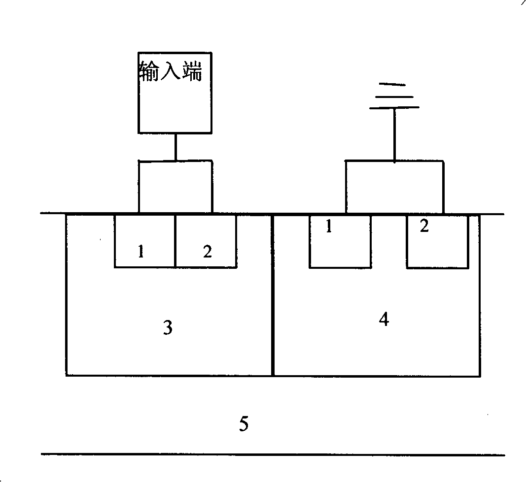
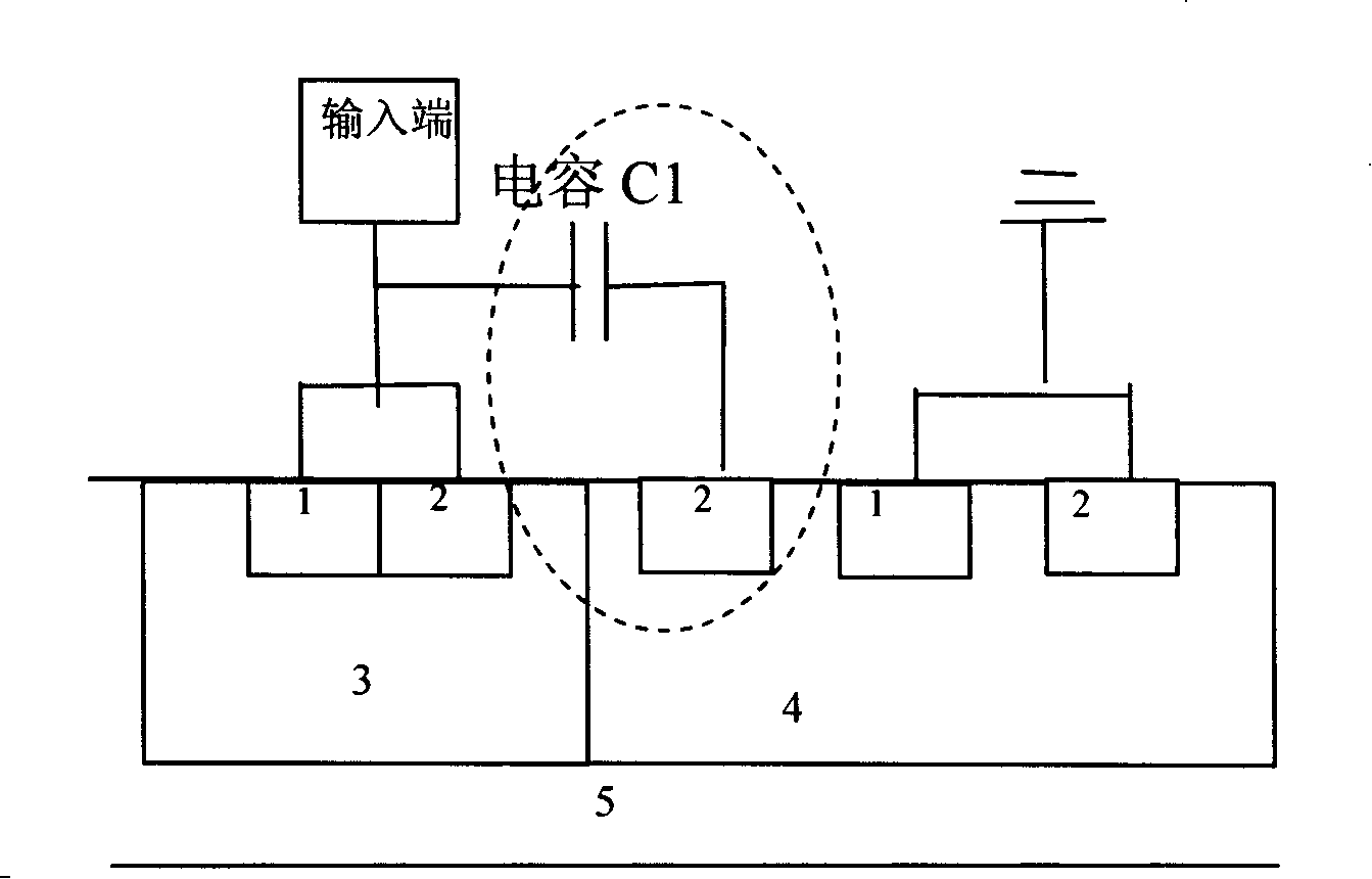
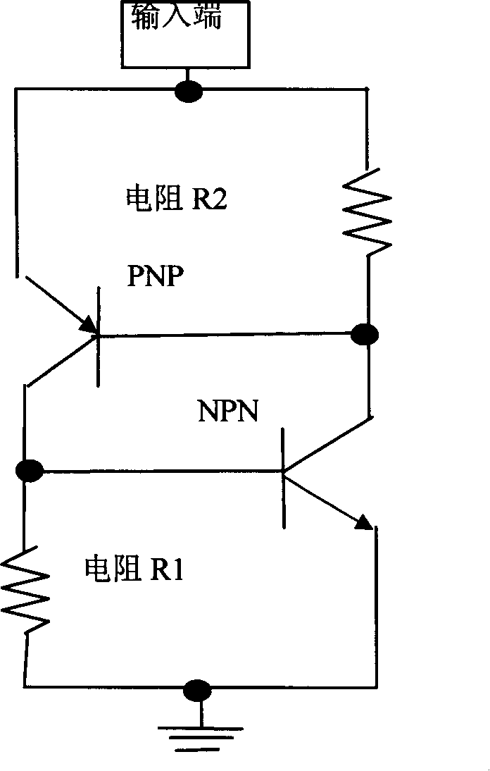
[0017] Such as figure 2 Shown is a schematic structural diagram of a specific embodiment of the present invention, in which: 1 is an N-type implanted region, 2 is a P-type implanted region, 3 is an N-well implanted region, 4 is a P-well implanted region, and 5 is a P-type substrate . The SCR in this embodiment still includes a P-N-P-N four-layer semiconductor structure, but in consideration of the above-mentioned principles of the invention, this embodiment is figure 1 After adding a P-type implant area and a capacitor C1 (100 picofarads) to the P well (PWell) shown, as Figure 5 As shown, the C1 capacitor and R1 resistance will form an RC coupling, which can provide a trigger signal to the base of the NPN during the process of static electricity, making the SCR structure easier to trigger earlier, that is: the trigger signal uses a capacitor and a resistor to form an RC circuit When there is ESD charge in the input terminal, the P-type injection area will have charge induction, ...


PUM


Abstract

The invention discloses an SCR electrostatic protection device and the manufacturing method thereof. The structure of the device comprises a P-type injection region (2) in a P well (4), an N-type injection region (1) in the P well (4), a P-type injection region (2) in an N well (3) and an N-type injection well (1) in the N well (3), and the P well is added with the P-type injection region (2), and a capacitance is arranged between the input terminal and the added P-type injection region. by adding the P-type injection region and the capacitance in the P well of the traditional SCR structure, the invention can reduce the turn-on voltage of the silicon controlled rectifier effectively without affecting protection ability, and the SCR structure is earlier and easier to be triggered, thus achieving better electrostatic protection effect.

Description

Technical field [0001] The invention relates to a semiconductor electrostatic protection technology, in particular to an SCR (Silicon Controlled Rectifier, silicon controlled rectifier) ​​electrostatic protection device and a manufacturing method. Background technique [0002] At present, SCRs are widely used as electrostatic discharge (ESD, Electrostatic Discharge) protection devices in semiconductor electrostatic protection. Such as figure 1 Shown is a schematic diagram of the structure of a commonly used SCR. The PNPN is composed of the P-type implanted region in the P-well, the N-type implanted region in the P-well, the P-type implanted region in the N-well, and the N-type implanted region in the N-well. Four-layer semiconductor structure. image 3 Is the equivalent circuit of the above-mentioned commonly used SCR, such as image 3 As shown, the coupling of the parasitic NPN and the parasitic PNP transistor will be formed, and when static electricity arrives and reaches a ce...

Claims


Application Information

Patent Timeline
Patent Type & Authority Applications(China)
IPC IPC(8): H01L27/04H01L23/60
Inventor 徐向明
Owner SHANGHAI HUA HONG NEC ELECTRONICS
Why Eureka
Try Eureka