Circuit board forming method and circuit board

A molding method and circuit board technology, which is applied in the direction of printed circuit, printed circuit manufacturing, electrical components, etc., can solve the problems of circuit board large shape tolerance, circuit board scrapping, etc., and achieve the effect of reducing shape tolerance and precise control

Active Publication Date: 2015-10-07
NEW FOUNDER HLDG DEV LLC
View PDF7 Cites 2 Cited by
  • Summary
  • Abstract
  • Description
  • Claims
  • Application Information

AI Technical Summary

Problems solved by technology

[0005] After the phenomenon of expansion and contraction offset occurs, if the traditional circuit board forming method is used to process each set of boards, then if figure 2 As shown, the circuit board will have a large shape tolerance, and if the shape tolerance exceeds a certain range, the circuit board will be scrapped

Method used


Image

  • Circuit board forming method and circuit board
  • Circuit board forming method and circuit board
  • Circuit board forming method and circuit board

Examples


Embodiment Construction

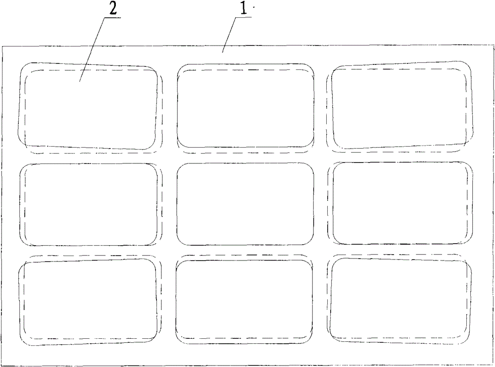
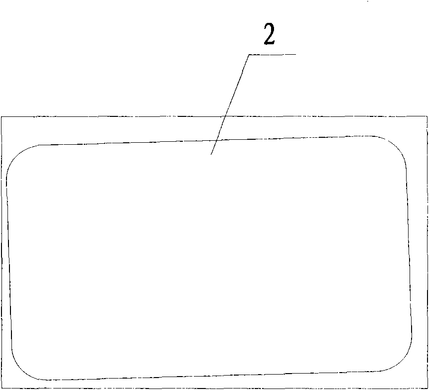
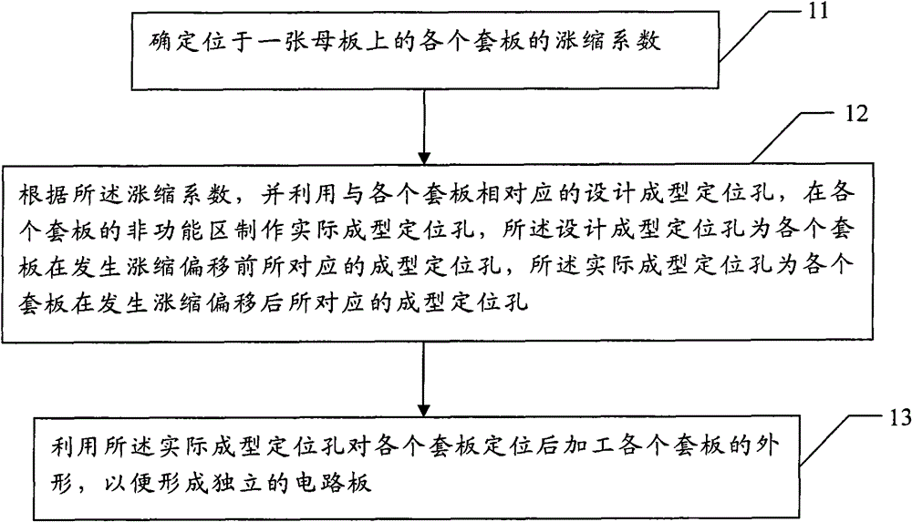
[0021] The invention provides a method for forming a circuit board, which is characterized in that it comprises:

[0022] Step 11, determining the expansion and contraction coefficients of each cover plate located on a motherboard;

[0023] Step 12, according to the expansion and contraction coefficients, and using the designed and formed positioning holes or designed and formed positioning parts corresponding to each cover plate, the actual forming positioning hole or the actual forming positioning part is made in the non-functional area of ​​each cover plate, the said The designed forming positioning hole or the designed forming positioning part is the corresponding forming positioning hole or forming positioning part of each cover board before expansion and contraction offset occurs, and the actual forming positioning hole or actual forming positioning part is the expansion and shrinkage of each cover plate. The corresponding forming positioning hole or forming positioning ...


PUM


Abstract

The invention discloses a circuit board forming method and a circuit board, relates to the technical field of circuit board manufacturing, and aims to reduce contour tolerances of the circuit board. The circuit board forming method comprises the following steps of: 11, determining expansion-contract coefficients of every sleeve plate on a motherboard; 12, according to the expansion-contract coefficients, forming an actual forming positioning hole in a non-functional area of each sleeve plate by using a design forming positioning hole or a design forming positioning part corresponding to each sleeve plate, wherein the design forming positioning hole is a forming positioning hole corresponding to each sleeve plate before expansion-contract deflection of each sleeve plate, and the actual forming positioning hole is a forming positioning hole corresponding to each sleeve plate after the expansion-contract deflection of each sleeve plate; and 13, processing the contour of each sleeve plate after positioning each sleeve plate by using the actual forming positioning hole so as to form an independent circuit board. The circuit board forming method disclosed by the invention can be used for forming processing of the circuit board.

Description

technical field [0001] The invention relates to the technical field of circuit board production, in particular to a circuit board forming method and the circuit board. Background technique [0002] When making circuit boards, in order to save production time and cost, generally multiple circuit boards are produced together on a large motherboard. When the insulating layer is used, the insulating layers of the plurality of circuit boards can be formed at one time. In this way, the motherboard contains multiple small sets of boards, and each set of boards can also contain one or more separate circuit boards. When the set of boards contains only one single circuit board, the set of boards can also be It is called a circuit board, and after the motherboard is produced, it is cut to separate each set of boards to form an independent set of boards. Afterwards, the circuit board molding process is performed, that is, the shape of each independent cover board is processed so as to...

Claims


Application Information

Patent Timeline
Patent Type & Authority Patents(China)
IPC IPC(8): H05K3/00H05K1/00
Inventor 朱兴华苏新虹
Owner NEW FOUNDER HLDG DEV LLC
Why Eureka
Try Eureka