PCB board-mounted resistor with polygonal cross-section and its forming process

A PCB board and molding process technology, applied in the field of PCB on-board resistors and their molding processes, can solve the problems of resistance row density and performance impact, poor resistance consistency and stability, and low resistance edge resolution. Regularity and controllability, improving consistency and stability, preserving the effect of appearance integrity

Active Publication Date: 2022-06-21
QUZHOU SUNLORD CIRCUIT BOARD CO LTD
View PDF4 Cites 0 Cited by
  • Summary
  • Abstract
  • Description
  • Claims
  • Application Information

AI Technical Summary

Problems solved by technology

Because the edge of the resistance of this type of cross-section is too thin, it leads to problems such as low imaging resolution and easy damage during processing, which makes the cross-sectional area of ​​the resistance discontinuous, the resistance consistency and stability of the resistance value are poor, and the resistance reliability is low.
At the same time, when such resistors are integrated to form an onboard resistor bank, the resolution of the resistor edge is not high, which affects the density and performance of the resistor bank

Method used


Image

  • PCB board-mounted resistor with polygonal cross-section and its forming process
  • PCB board-mounted resistor with polygonal cross-section and its forming process
  • PCB board-mounted resistor with polygonal cross-section and its forming process

Examples


specific Embodiment 1

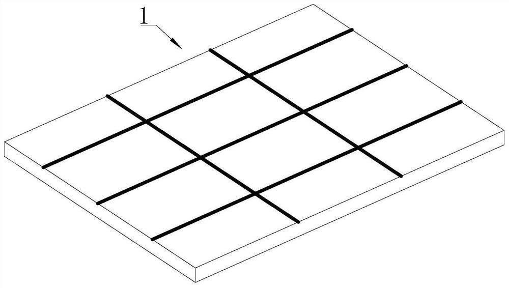
[0052] Specific embodiment 1: please refer to Figure 1-11 , including the following steps:

[0053] A. Provide a base plate 1. The upper and lower end surfaces of the base plate 1 are provided with a plurality of transverse folding block lines and a plurality of longitudinal folding lines. The polylines and polyblocks are crisscrossed to form multiple grids. The position of the fold line on the lower end face corresponds to the position of the fold line on the upper end face. The grid areas on the upper end face correspond one-to-one with the grid areas on the lower end face. The position of the folded block line on the lower end face corresponds to the position of the folded block line on the upper end face.

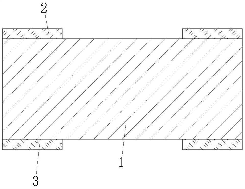
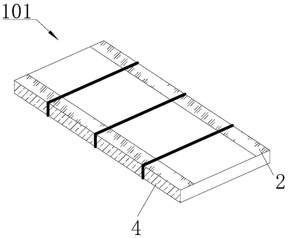
[0054] B. The electrode paste is printed on the substrate 1 by screen printing on the upper end surface of the substrate 1 , and the front electrode 2 is formed after drying and sintering. There are two front electrodes 2 in each grid area. The two front electrode...

specific Embodiment 2

[0065] Specific embodiment 2: different from specific embodiment 1, please refer to Figure 12-13 , the cross section of the resistance core 6 is T-shaped, and the outer side of the resistance core 6 is attached to the inner end and part of the upper end of the front electrode 2, so that the cross section of the finally formed resistance layer 6 is also T-shaped, effectively ensuring resistance The connection area between the layer 6 and the front electrode can effectively prevent the PCB resistance from being disconnected from the front electrode 2 due to the bending of the resistance layer 6 between the two front electrodes 2 after the expansion of heat and heat.

specific Embodiment 3

[0066] Specific embodiment 3: Different from the specific embodiment 1, the resistance core 6 and the resistance mold 7 are both sintered from sodium chloride solid, and the sintered core and the mold 7 are polished by laser to control the shape and the inner cavity. flatness.


PUM


Abstract

The invention discloses a PCB board-mounted resistor with a polygonal cross-section and a molding process thereof, belonging to the field of electrical component manufacturing. The PCB on-board resistor forming process with polygonal cross-section includes the following steps: A. A substrate is provided, and a plurality of horizontal folding lines and a plurality of longitudinal folding lines are provided on the upper end surface and the lower end surface of the substrate. The folding line and the folding block line cross each other to form a plurality of grid areas. The position of the fold line on the lower end face corresponds to the position of the fold line on the upper end face one by one. The grid area on the upper end face corresponds to the grid area on the lower end face one by one. The position of the folded line on the lower end surface corresponds to the position of the folded line on the upper end face one by one. It can realize the PCB resistor with a polygonal resistance layer, increase the edge thickness of the onboard resistance, and improve the regularity and controllability of the geometric shape of the resistance section. In order to improve the consistency and stability of the resistance value of the resistance, and improve the reliability of the resistance at the same time.

Description

technical field [0001] The invention belongs to the field of printed circuit technology, and more particularly, relates to a PCB on-board resistor with a polygonal section and a forming process thereof. Background technique [0002] PCB on-board resistors are mainly made of substrates, resistive films, protective films, electrodes and other materials. [0003] The substrate mainly includes an alumina ceramic body. The two sides of the upper surface of the alumina ceramic body are respectively printed with back electrodes, the two sides of the lower surface are respectively printed with front electrodes, and resistors are printed on the upper surface of the alumina ceramic body between the two back electrodes. The two sides of the alumina ceramic body are provided with side electrodes, so that the front electrodes are connected to the back electrodes, and the back electrodes, the front electrodes and the side electrodes are plated with protective layers. [0004] Because the...

Claims


Application Information

Patent Timeline
Patent Type & Authority Patents(China)
IPC IPC(8): H01C17/065H01C17/28H01C17/30
CPCH01C17/06533H01C17/281H01C17/288H01C17/30
Inventor 石林国陆云鹏姜玉晋黄根华袁琛徐利刚廖君孙明海
Owner QUZHOU SUNLORD CIRCUIT BOARD CO LTD
Why Eureka
Try Eureka