Laminated inverted chip packaging structure of ultra-fine spacing welding plates and bottom filling material preparation method
A flip-chip, packaging structure technology, applied in semiconductor/solid-state device manufacturing, semiconductor/solid-state device components, semiconductor devices, etc., and can solve problems such as difficulty in implementation
- Summary
- Abstract
- Description
- Claims
- Application Information
AI Technical Summary
Problems solved by technology
Method used
Image

Examples
Embodiment Construction
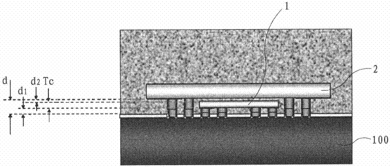
[0038] Spatially relative terms such as "beneath," "lower," "above," "upper," etc. may be used herein to readily describe an element or feature shown in the figures in relation to other elements. or feature relations. It will be understood that the spatially relative terms are intended to encompass different orientations of the device in use or operation in addition to the orientation depicted in the figures. For example, if the device in the figures is turned over, elements described as "below" or "beneath" other elements or features would then be oriented "above" the other elements or features. Thus, the exemplary term "below" can encompass both an orientation of "above" and "beneath". The device may be at other orientations (rotated 90 degrees or at other orientations) and the spatially relative descriptors used herein should be interpreted accordingly.
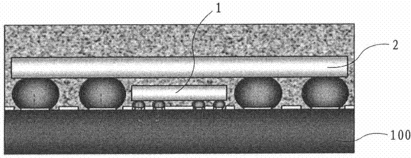
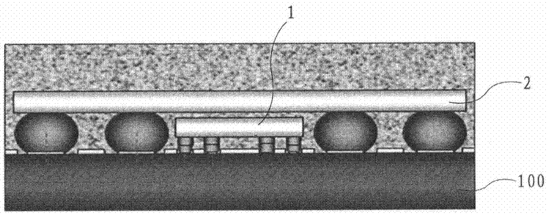
[0039] Hereinafter, embodiments of the present invention will be described in detail with reference to the drawings. ...
PUM
 Abstract
Description
Claims
Application Information